Comparator (COMP) RM0440
778/2126 RM0440 Rev 4
24 Comparator (COMP)
24.1 COMP introduction
The device embeds up to seven ultra-fast analog comparators.
The comparators can be used for a variety of functions including:
• Wake-up from low-power mode triggered by an analog signal,
• Analog signal conditioning,
• Cycle-by-cycle current control loop when combined with a PWM output from a timer.
24.2 COMP main features
• Each comparator has configurable plus and minus inputs used for flexible voltage
selection:
– Multiplexed I/O pins
– DAC channels
– Internal reference voltage and three submultiple values (1/4, 1/2, 3/4) provided by
a scaler (buffered voltage divider)
• Programmable hysteresis
• Output redirection to I/Os or to timer inputs for triggering break events for fast PWM
shutdowns
• Output blanking for immunity to switching noise
• Per-channel interrupt generation with wake-up from Sleep and Stop modes
24.3 COMP functional description
24.3.1 COMP block diagram
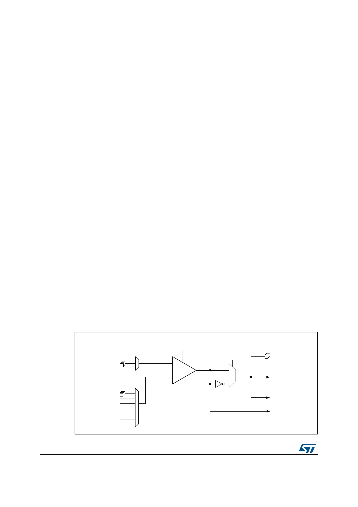
The block diagram of one comparator channel front-end is shown in Figure 168:
Comparator block diagram.
Figure 168. Comparator block diagram
MSv47930V3
COMPx_INM I/Os
1/4 V
REFINT
3/4 V
REFINT
1/2 V
REFINT
V
REFINT
DACx_OUTy
DACx_OUTy
COMPx_INP
COMPx_INM
Wakeup EXTI line
interrupt
Polarity selection
POLARITY
VALUE
COMPx_OUT
INMSEL
GPIO
alternate
function
+
-
COMPx
INPSEL
COMPx_INP I/Os
HYST
TIMx
HRTIM
 Loading...


