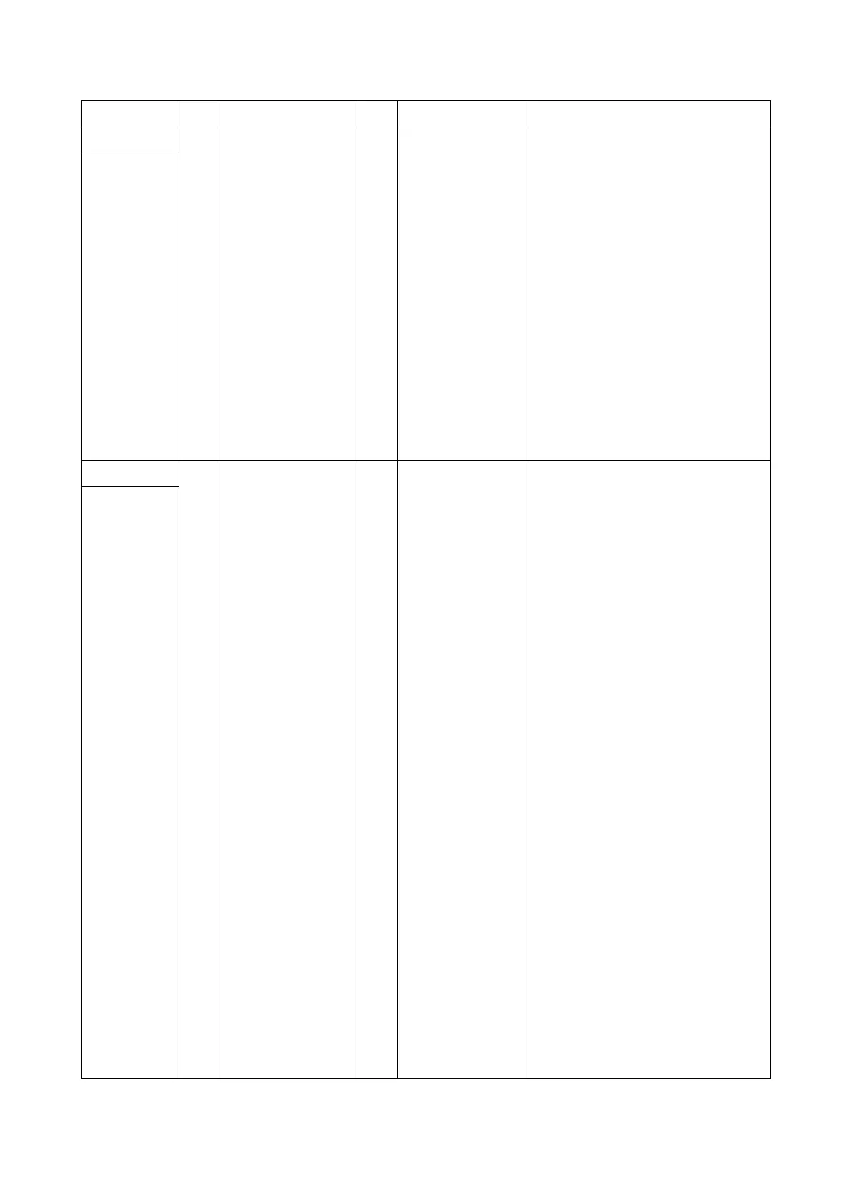
2N8/2N7
2-3-86
YC4_A A1 ANODE O 3.3 V DC 3.3 V DC power output to DPLS1
Connected to
DP lift sen-
sor 1, DP
feed sensor,
DP eject
sensor
A2 GND - - Ground
A3 LF_UPSW I 0/3.3 V DC DPLS1: On/Off
A4 GND - - Ground
A5 FD_SW I 0/3.3 V DC DPFS: On/Off
A6 3.3V O 3.3 V DC 3.3 V DC power output to DPFS
A7 NC - - Not used
A8 NC - - Not used
A9 NC - - Not used
A10 ANODE O 3.3 V DC 3.3 V DC power output to DPES
A11 GND - - Ground
A12 EXIT_SW(M) I 0/3.3 V DC DPES: On/Off
A13 NC - - Not used
YC4_B B1 NC - - Not used
Connected to
DPLED
PWB, DP
timing sen-
sor, DP open/
close switch
B2 LED_PW O 5.6 V DC 5.6 V DC power output to LEDPWB
B3 LED_REM O 0/5.6 V DC LED control signal
B4 NC(GND) - - Not used
B5 GND - - Ground
B6 CCD_TMG_SW I 0/3.3 V DC DPTS: On/Off
B7 3.3V O 3.3 V DC 3.3 V DC power output to DPTS
B8 ANODE O 3.3 V DC 3.3 V DC power output to DPOCSW
B9 GND - - Ground
B10 DP_OPEN I 0/3.3 V DC DPOCSW: On/Off
B11 ANODE - - Not used
B12 GND - - Not used
B13 SKEW_SW - - Not used
Connector Pin Signal I/O Voltage Description
 Loading...