Type No. Terminal Name (Function) Function (Signal Level) Default Setting
Main Frequency
Reference Input
RP Multi-function pulse train input (frequency reference)
Response frequency: 0.5 to 32 kHz
(Duty Cycle: 30 to 70%)
(High level voltage: 3.5 to 13.2 Vdc)
(Low level voltage: 0.0 to 0.8 Vdc)
(input impedance: 3 kΩ)
+V Analog input power supply +10.5 Vdc (max allowable current 20 mA)
A1 Multi-function analog input (frequency reference) Input voltage 0 to +10 Vdc (20 kΩ) resolution1/1000
A2 Multi-function analog input (frequency reference)
Input voltage or input current (Selected by DIP switch S1) 0 to +10 Vdc (20 kΩ),
Resolution: 1/1000
4 to 20 mA (250 Ω) or 0 to 20 mA (250 Ω), Resolution: 1/500
AC Frequency reference common 0 Vdc
n
Output Terminals
Table 3.7 Control Circuit Output Terminals
Type No. Terminal Name (Function) Function (Signal Level)Default Setting
Multi-Function Digital Output
MA N.O. (fault)
Digital output
30 Vdc, 10 mA to 1 A; 250 Vac, 10 mA to 1 A
Minimum load: 5 Vdc, 10 mA (reference value)
MB N.C. output (fault)
MC Digital output common
Multi-Function Photocoupler
Output
P1 Photocoupler output 1 (during run)
Photocoupler output 48 Vdc, 2 to 50 mAP2 Photocoupler output 2 (Frequency agree)
PC Photocoupler output common
Monitor Output
MP Pulse train output (input frequency) 32 kHz (max)
AM Analog monitor output 0 to 10 Vdc (2 mA or less) Resolution: 1/1000
AC Monitor common 0 V
Connect a suppression diode as shown in Figure 3.19 when driving a reactive load such as a relay coil. Ensure the diode rating is greater than the circuit
voltage.
A
B
C
D
A – External power, 48 V max.
B – Suppression diode
C – Coil
D – 50 mA or less
Figure 3.19 Connecting a Suppression Diode
n
Serial Communication Terminals
Table 3.8 Control Circuit Terminals: Serial Communications
Type No. Signal Name Function (Signal Level)
MEMOBUS/Modbus
Communication
R+ Communications input (+)
MEMOBUS/Modbus communication: Use a RS-485 or
RS-422 cable to connect the drive.
RS-485/422 MEMOBUS/
Modbus communication
protocol 115.2 kbps (max.)
R- Communications input (-)
S+ Communications output (+)
S- Communications output (-)
IG Shield ground 0 V
u
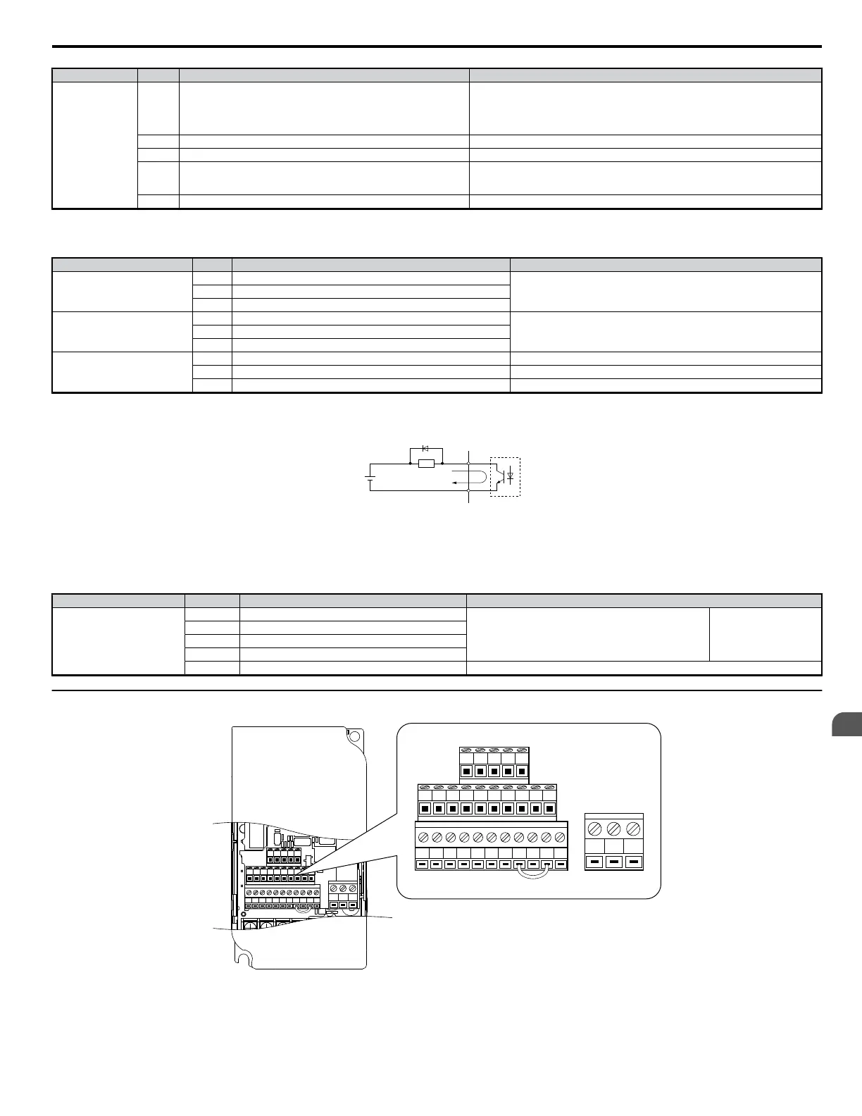
Removable Terminal Block Configuration
S1 S2 S3 S4 S5 S6 S7 HC SC H1 RP
R+ R– S+ S– IG
P1 P2 PC A1 A2 +V AC AM AC MP
MCMBMA
S1 S2 S3 S4 S5 S6 S7 HC SC H1 RP
R+ R- S+ S- IG
P1 P2 PC A1 A2 +V AC AM AC MP
MCMBMA
Figure 3.20 Removable Control Circuit Terminal Block
(CIMR-VAoooooooo; CIMR-VUoooooooooo)
3.7 Control Circuit Wiring
YASKAWA ELECTRIC SIEP C710606 18A YASKAWA AC Drive – V1000 Technical Manual (Preliminary)
45
3
Electrical Installation
 Loading...