Analog-to-digital converters (ADC) RM0440
716/2126 RM0440 Rev 4
21.7 ADC common registers
These registers define the control and status registers common to master and slave ADCs:
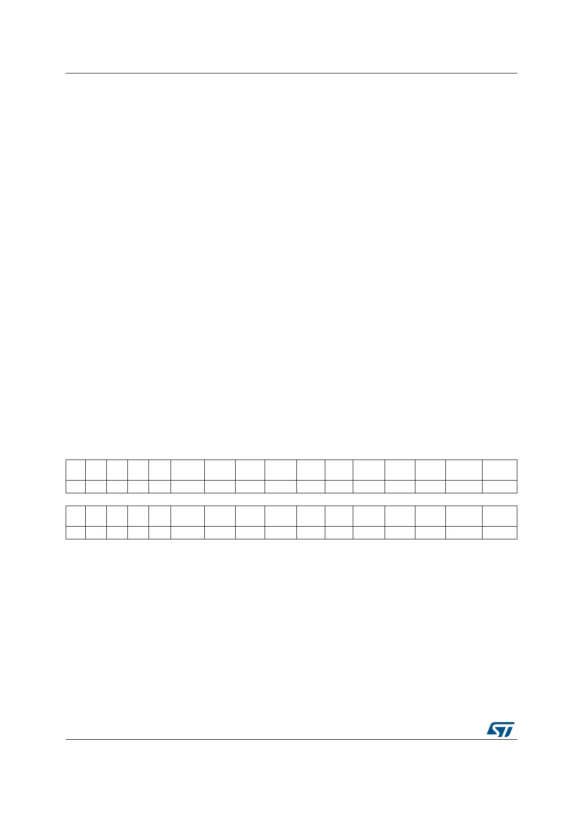
21.7.1 ADCx common status register (ADCx_CSR) (x=12 or 345)
Address offset: 0x00 (this offset address is relative to the master ADC base address +
0x300)
Reset value: 0x0000 0000
This register provides an image of the status bits of the different ADCs. Nevertheless it is
read-only and does not allow to clear the different status bits. Instead each status bit must
be cleared by writing 0 to it in the corresponding ADC_ISR register.
One interface controls ADC1 and ADC2, while the other interface controls ADC3, ADC4 and
ADC5.
Bits 31:14 Reserved, must be kept at reset value.
Bits 13:0 GCOMPCOEFF[13:0]: Gain compensation coefficient
These bits are set and cleared by software to program the gain compensation coefficient.
00 1000 0000 0000: gain factor of 0.5
...
01 0000 0000 0000: gain factor of 1
10 0000 0000 0000: gain factor of 2
11 0000 0000 0000: gain factor of 3
...
The coefficient is divided by 4096 to get the gain factor ranging from 0 to 3.999756.
Note: This gain compensation is only applied when GCOMP bit of ADC_CFGR2 register is 1.
31 30 29 28 27 26 25 24 23 22 21 20 19 18 17 16
Res. Res. Res. Res. Res.
JQOVF_
SLV
AWD3_
SLV
AWD2_
SLV
AWD1_
SLV
JEOS_
SLV
JEOC_
SLV
OVR_
SLV
EOS_
SLV
EOC_
SLV
EOSMP_
SLV
ADRDY_
SLV
rrrrrrrrr r r
15 14 13 12 11 10 9 8 7 6 5 4 3 2 1 0
Res. Res. Res. Res. Res.
JQOVF_
MST
AWD3_
MST
AWD2_
MST
AWD1_
MST
JEOS_
MST
JEOC_
MST
OVR_
MST
EOS_
MST
EOC_
MST
EOSMP_
MST
ADRDY_
MST
rrrrrrrrr r r
Bits 31:27 Reserved, must be kept at reset value.
Bit 26 JQOVF_SLV: Injected Context Queue Overflow flag of the slave ADC
This bit is a copy of the JQOVF bit in the corresponding ADC_ISR register.
Bit 25 AWD3_SLV: Analog watchdog 3 flag of the slave ADC
This bit is a copy of the AWD3 bit in the corresponding ADC_ISR register.
Bit 24 AWD2_SLV: Analog watchdog 2 flag of the slave ADC
This bit is a copy of the AWD2 bit in the corresponding ADC_ISR register.
Bit 23 AWD1_SLV: Analog watchdog 1 flag of the slave ADC
This bit is a copy of the AWD1 bit in the corresponding ADC_ISR register.
 Loading...


