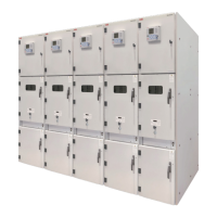
P
Q
Non
tripping
area
Tripping
area
P
Q
Tripping area
Non
tripping area
(a) (b)
GUID-8D2C91A5-4C25-4B40-8B67-8D3EBFD3D452 V1 EN
Figure 365: Reverse active overpower characteristics (a) and reverse reactive
overpower characteristics (b)
4.8.2.6 Signals
Table 630: 32R/32O Input signals
Name
Type Default Description
I_A SIGNAL 0 Phase A current
I_B SIGNAL 0 Phase B current
I_C SIGNAL 0 Phase C current
V_A SIGNAL 0 Phase-to-ground voltage A or phase-to-phase voltage
AB
V_B SIGNAL 0 Phase-to-ground voltage B or phase-to-phase voltage
BC
V_C SIGNAL 0 Phase-to-ground voltage C or phase-to-phase voltage
CA
BLOCK BOOLEAN 0=False Block signal for activating the blocking mode
Table 631: 32R/32O Output signals
Name
Type Description
TRIP BOOLEAN Trip
PICKUP BOOLEAN Pickup
1MAC059074-MB A Section 4
Protection functions
615 series ANSI 731
Technical Manual

 Loading...