CDM Application Example
PVIB/YVIB
PR1H
PR1L
2Vpp
12Vdc
2ms (500Hz)
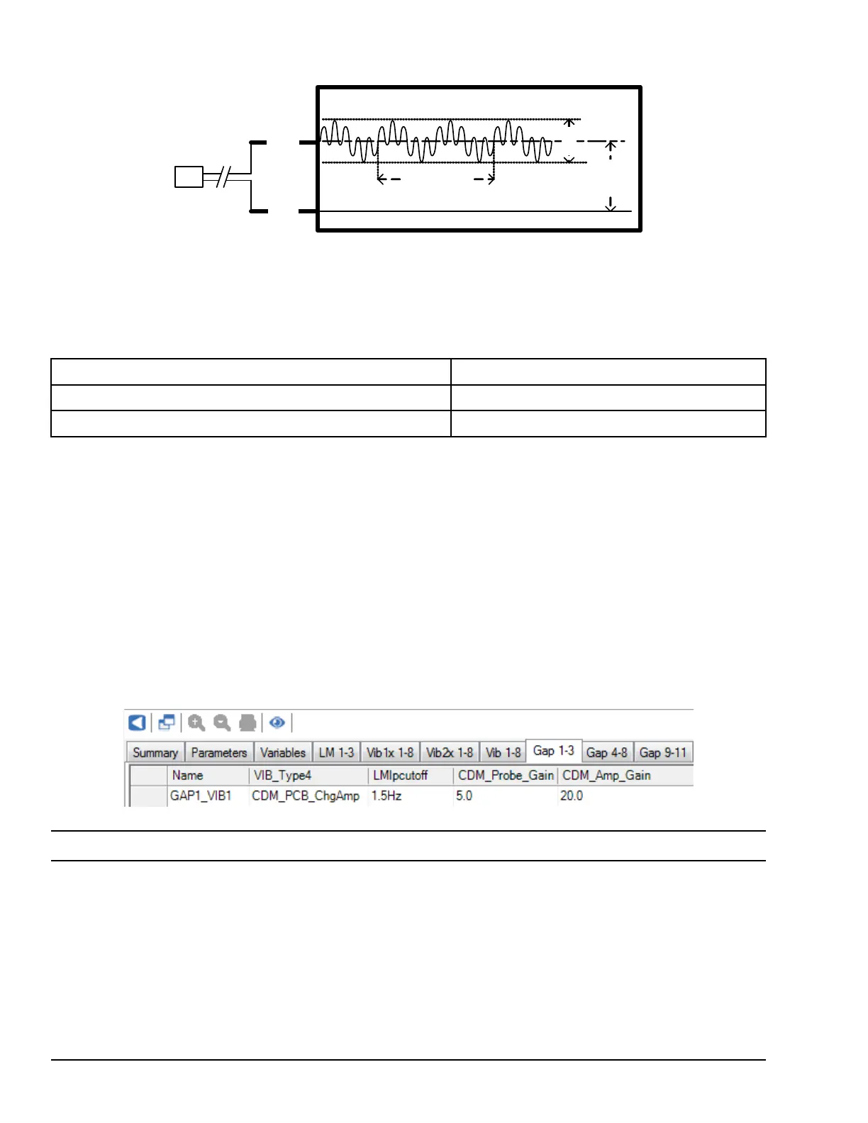
In this example, PCB CDM voltage inputs to a YVIB application are measured at the terminal board screws. Assume this
sensor is connected to Channel 1 as a CDM_PCB_ChgAmp input.
For this example, the input waveform is two 1 VPK-PK pure tones (500Hz sine wave and 2500Hz sine wave) summed
together. This is for illustrative purposes only, and is not indicative of true sensor inputs.
Example PCB Sensor Specifications
PCB Probe Gain 5.0 pC/PSI
PCB Amp Gain 20.0 mV/pC
Frequency Response 200 Hz – 4 kHz
We will configure Channel 1 for the following behaviors:
• Utilize the RMS Dynamic Pressure algorithm for computing VIB1 signal.
• Return VIB1 signal in PSI.
• Apply 10-pole low-pass and high-pass wideband filters to pass only inputs within PCB Sensor frequency response.
• Utilize LM_RPM_A to return LMVib1A as Peak Dynamic Pressure at 2500 Hz (150000 RPM = 2500 Hz * 60 RPM / Hz)
with a filter bandwidth of 3Hz.
• Set CDM_Scan_Period to 640 ms
➢➢ To configure Channel 1
1. From the Parameters tab, set OperatingMode to Enhanced and set CDM_Scan_Period to 640 ms.
2. From the Gap 1-3 tab, select GAP1_VIB1 and make the following configuration changes as displayed in the following
screen.
Note These parameters will appear when a CDM sensor is selected in the VIB_Type parameter.
3. Navigate to the Vib 1-8 tab. Select VIB1. Click to Show Advanced Parameters.
260 GEH-6855_Vol_II GEH-6855_Vol_II Mark VIeS Functional Safety Systems Volume II
Public Information