10.4.2 Operation
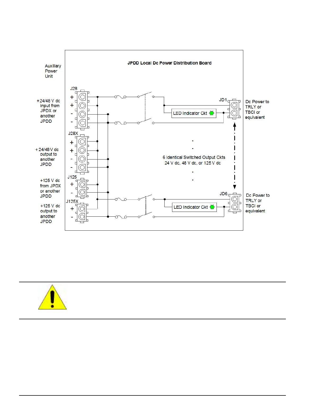
The following figure explains how the 125 V dc, 48 V dc, or 24 V dc power is distributed in JPDD, and how it reaches the
TRLY and TBCI boards.
JPDD Simplified Circuit Diagram
10.4.2.1 Inputs
Multiple JPDD boards can receive power from a single Main Power Distribution Module branch circuit. Power input can be
either 125 V dc, 48 V dc, or 24 V dc nominal.
Caution
Both inputs share a common electrical path. Only a single voltage (24, 48, or 125) can
be applied at one time to both inputs.
Two 2-Pin Mate-N-Lok connectors are provided for 125 V dc power. One connector receives input power and the other can
be used to distribute 125 V dc power to another JPDD board in daisy chain fashion.
Two 4-pin Mate-N-Lok connectors are provided for 24/48 V dc power. These perform functions similar to those of the 2-pin
connectors above. The 4-pin connector permits parallel connection of two pin-pairs for increased current capacity. It is
expected that neither side of the dc power input is grounded.
364 GEH-6855_Vol_II GEH-6855_Vol_II Mark VIeS Functional Safety Systems Volume II
Public Information


 To Next Page