Flexible static memory controller (FSMC) RM0440
552/2126 RM0440 Rev 4
SRAM/NOR-Flash chip-select timing register for bank x (FMC_BTRx)
Address offset: 0x04 + 8 * (x – 1), (x = 1 to 4)
Reset value: 0x0FFF FFFF
This register contains the control information of each memory bank, used for SRAMs,
PSRAM and NOR Flash memories.If the EXTMOD bit is set in the FMC_BCRx register, then
this register is partitioned for write and read access, that is, 2 registers are available: one to
configure read accesses (this register) and one to configure write accesses (FMC_BWTRx
registers).
Bits 3:2 MTYP[1:0]: Memory type
Defines the type of external memory attached to the corresponding memory bank.
00: SRAM/FRAM (default after reset for Bank 2...4)
01: PSRAM (CRAM) / FRAM
10: NOR Flash/OneNAND Flash (default after reset for Bank 1)
11: reserved
Bit 1 MUXEN: Address/data multiplexing enable bit
When this bit is set, the address and data values are multiplexed on the data bus, valid only with
NOR and PSRAM memories:
0: Address/data non multiplexed
1: Address/data multiplexed on databus (default after reset)
Bit 0 MBKEN: Memory bank enable bit
Enables the memory bank. After reset Bank1 is enabled, all others are disabled. Accessing a
disabled bank causes an ERROR on AHB bus.
0: Corresponding memory bank is disabled.
1: Corresponding memory bank is enabled.
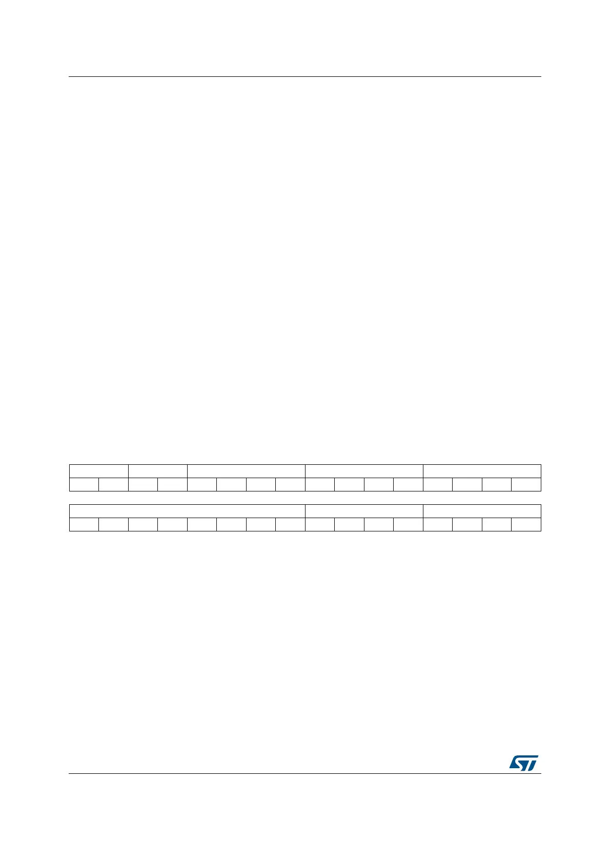
31 30 29 28 27 26 25 24 23 22 21 20 19 18 17 16
DATAHLD[1:0] ACCMOD[1:0] DATLAT[3:0] CLKDIV[3:0] BUSTURN[3:0]
rw rw rw rw rw rw rw rw rw rw rw rw rw rw rw rw
1514131211109876543210
DATAST[7:0] ADDHLD[3:0] ADDSET[3:0]
rw rw rw rw rw rw rw rw rw rw rw rw rw rw rw rw
Bits 31:30 DATAHLD[1:0]: Data hold phase duration
These bits are written by software to define the duration of the data hold phase in HCLK
cycles (refer to Figure 54 to Figure 66), used in asynchronous accesses:
For read accesses
00: DATAHLD phase duration = 0 × HCLK clock cycle (default)
01: DATAHLD phase duration = 1 × HCLK clock cycle
10: DATAHLD phase duration = 2 × HCLK clock cycle
11: DATAHLD phase duration = 3 × HCLK clock cycle
For write accesses
00: DATAHLD phase duration = 1 × HCLK clock cycle (default)
01: DATAHLD phase duration = 2 × HCLK clock cycle
10: DATAHLD phase duration = 3 × HCLK clock cycle
11: DATAHLD phase duration = 4 × HCLK clock cycle
 Loading...


