Quad-SPI interface (QUADSPI) RM0440
594/2126 RM0440 Rev 4
20.5.6 QUADSPI communication configuration register (QUADSPI_CCR)
Address offset: 0x0014
Reset value: 0x0000 0000
Bits 31:0 DL[31:0]: Data length
Number of data to be retrieved (value+1) in indirect and status-polling modes. A value
no greater than 3 (indicating 4 bytes) should be used for status-polling mode.
All 1s in indirect mode means undefined length, where QUADSPI will continue until the
end of memory, as defined by FSIZE.
0x0000_0000: 1 byte is to be transferred
0x0000_0001: 2 bytes are to be transferred
0x0000_0002: 3 bytes are to be transferred
0x0000_0003: 4 bytes are to be transferred
...
0xFFFF_FFFD: 4,294,967,294 (4G-2) bytes are to be transferred
0xFFFF_FFFE: 4,294,967,295 (4G-1) bytes are to be transferred
0xFFFF_FFFF: undefined length -- all bytes until the end of Flash memory (as defined
by FSIZE) are to be transferred. Continue reading indefinitely if FSIZE = 0x1F.
DL[0] is stuck at ‘1’ in dual-flash mode (DFM = 1) even when ‘0’ is written to this bit, thus
assuring that each access transfers an even number of bytes.
This field has no effect when in memory-mapped mode (FMODE = 10).
This field can be written only when BUSY = 0.
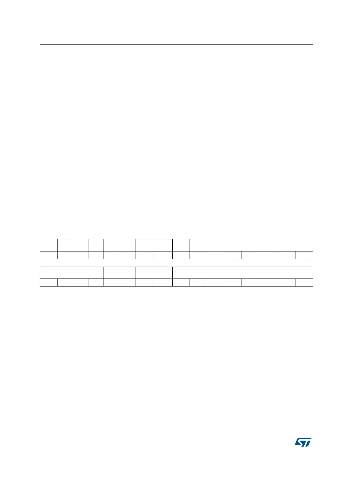
31 30 29 28 27 26 25 24 23 22 21 20 19 18 17 16
DDRM DHHC Res. SIOO FMODE[1:0] DMODE[1:0] Res. DCYC[4:0] ABSIZE[1:0]
rw rw rw rw rw rw rw rw rw rw rw rw rw rw
15 14 13 12 11 10 9 8 7 6 5 4 3 2 1 0
ABMODE[1:0] ADSIZE[1:0] ADMODE[1:0] IMODE[1:0] INSTRUCTION[7:0]
rw rw rw rw rw rw rw rw rw rw rw rw rw rw rw rw
Bit 31 DDRM: Double data rate mode
This bit sets the DDR mode for the address, alternate byte and data phase:
0: DDR Mode disabled
1: DDR Mode enabled
This field can be written only when BUSY = 0.
Bit 30 DHHC: DDR hold
Delay the data output by 1/4 of the QUADSPI output clock cycle in DDR mode:
0: Delay the data output using analog delay
1: Delay the data output by 1/4 of a QUADSPI output clock cycle.
This feature is only active in DDR mode.
This field can be written only when BUSY = 0.
Note: PRESCALER>0 is mandatory when DHHC=1.
Bit 29 Reserved, must be kept at reset value.
 Loading...