Analog-to-digital converters (ADC) RM0440
708/2126 RM0440 Rev 4
Note: Some channels are not connected physically and must not be selected for conversion.
21.6.15 ADC regular data register (ADC_DR)
Address offset: 0x40
Reset value: 0x0000 0000
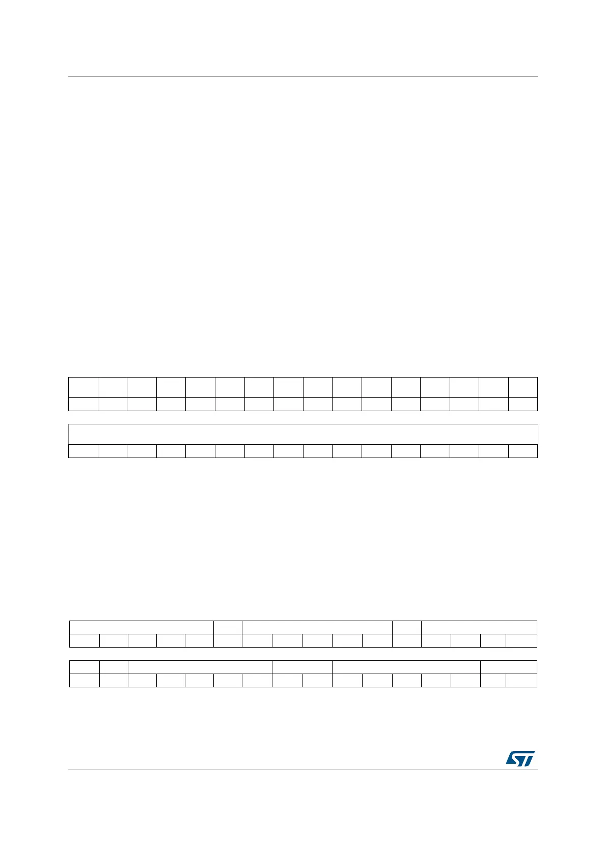
21.6.16 ADC injected sequence register (ADC_JSQR)
Address offset: 0x4C
Reset value: 0x0000 0000
Bits 31:11 Reserved, must be kept at reset value.
Bits 10:6 SQ16[4:0]: 16th conversion in regular sequence
These bits are written by software with the channel number (0 to 18) assigned as the 16th in
the regular conversion sequence.
Note: The software is allowed to write these bits only when ADSTART=0 (which ensures that
no regular conversion is ongoing).
Bit 5 Reserved, must be kept at reset value.
Bits 4:0 SQ15[4:0]: 15th conversion in regular sequence
These bits are written by software with the channel number (0 to 18) assigned as the 15th in
the regular conversion sequence.
Note: The software is allowed to write these bits only when ADSTART=0 (which ensures that
no regular conversion is ongoing).
31 30 29 28 27 26 25 24 23 22 21 20 19 18 17 16
Res. Res. Res. Res. Res. Res. Res. Res. Res. Res. Res. Res. Res. Res. Res. Res.
1514131211109876543210
RDATA[15:0]
rrrrrrrrrrrrrrrr
Bits 31:16 Reserved, must be kept at reset value.
Bits 15:0 RDATA[15:0]: Regular data converted
These bits are read-only. They contain the conversion result from the last converted regular channel.
The data are left- or right-aligned as described in Section 21.4.26: Data management.
31 30 29 28 27 26 25 24 23 22 21 20 19 18 17 16
JSQ4[4:0] Res. JSQ3[4:0] Res. JSQ2[4:1]
rw rw rw rw rw rw rw rw rw rw rw rw rw
15 14 13 12 11 10 9 8 7 6 5 4 3 2 1 0
JSQ20 Res. JSQ1[4:0] JEXTEN[1:0] JEXTSEL[4:0] JL[1:0]
rw rw rw rw rw rw rw rw rw rw rw rw rw rw rw
 Loading...


