CPU Specifications
and Operation
4–43
CPU Specifications and Operation
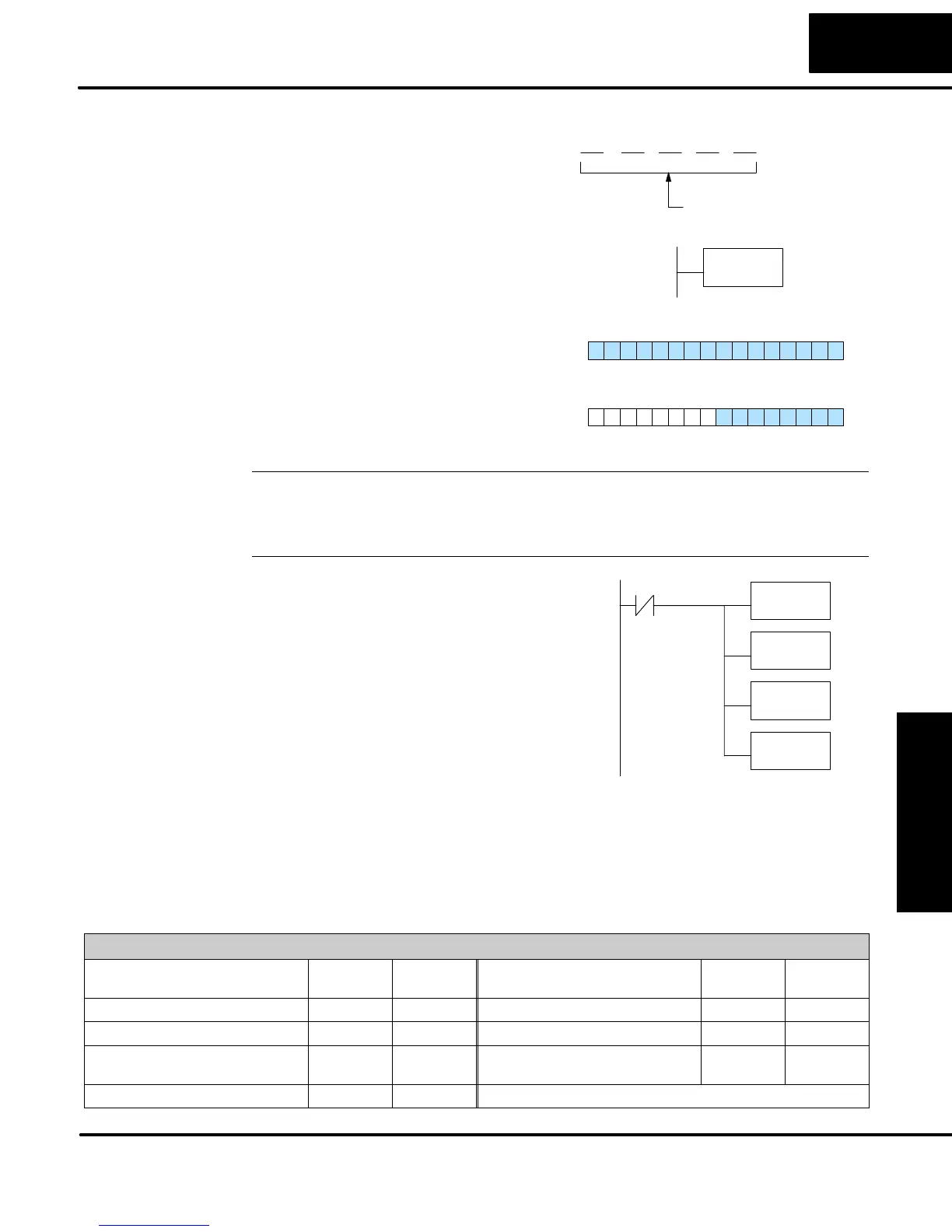
The third instruction in the RX or WX
sequence is a Load Address (LDA)
instruction. Its purpose is to load the
starting address of the memory area to be
transferred. Entered as an octal number,
the LDA instruction converts it to hex and
places the result in the accumulator.
For a WX instruction, the DL05 CPU
sends the number of bytes previously
specified from its memory area beginning
at the LDA address specified.
For an RX instruction, the DL05 CPU
reads the number of bytes previously
specified from the slave, placing the
received data into its memory area
beginning at the LDA address specified.
6 0 00
(octal)
LDA
O40600
4
Starting address of
master transfer area
V40600
MSB LSB
015
V40601
MSB LSB
015
NOTE: Since V memory words are always 16 bits, you may not always use the whole
word. For example, if you only specify 3 bytes and you are reading Y outputs from the
slave, you will only get 24 bits of data. In this case, only the 8 least significant bits of
the last word location will be modified. The remaining 8 bits are not affected.
The last instruction in our sequence is the
WX or RX instruction itself. Use WX to
write to the slave, and RX to read from the
slave. All four of our instructions are
shown to the right. In the last instruction,
you must specify the starting address and
a valid data type for the slave.
LD
KF201
LD
K64
LDA
O40600
RX
Y0
SP116
S DirectNET slaves – specify the same address in the WX and RX
instruction as the slave’s native I/O address
S MODBUS DL405, DL205, or DL05 slaves – specify the same address
in the WX and RX instruction as the slave’s native I/O address
S MODBUS 305 slaves – use the following table to convert DL305
addresses to MODBUS addresses
DL305 Series CPU Memory Type–to–MODBUS Cross Reference (excluding 350 CPU)
PLC Memory type PLC base
address
MODBUS
base addr.
PLC Memory Type PLC base
address
MODBUS
base addr.
TMR/CNT Current Values R600 V0 TMR/CNT Status Bits CT600 GY600
I/O Points IO 000 GY0 Control Relays CR160 GY160
Data Registers R401,
R400
V100 Shift Registers SR400 GY400
Stage Status Bits (D3–330P only) S0 GY200
Step 3:
Specify Master
Memory Area
Step 4:
Specify Slave
Memory Area