RL78/G10 CHAPTER 12 SERIAL ARRAY UNIT
R01UH0384EJ0311 Rev. 3.11 298
Dec 22, 2016
12.3.13 Serial clock output register 0 (CKO0)
The CKO0 register is a buffer register for serial clock output of each channel.
The value of the CKO0n bit of this register is output from the serial clock output pin of channel n.
The CKO0n bit of this register can be rewritten by software only when channel operation is disabled (SE0n = 0). When
channel operation is enabled (SE0n = 1), rewriting by software is ignored, and the value of the register can be changed
only by a serial communication operation.
To use the pin for serial interface as a port function pin, set the corresponding CKO0n bit to 1.
The CKO0 register can be set by an 8-bit memory manipulation instruction.
Reset signal generation clears the CKO0 register to 03H.
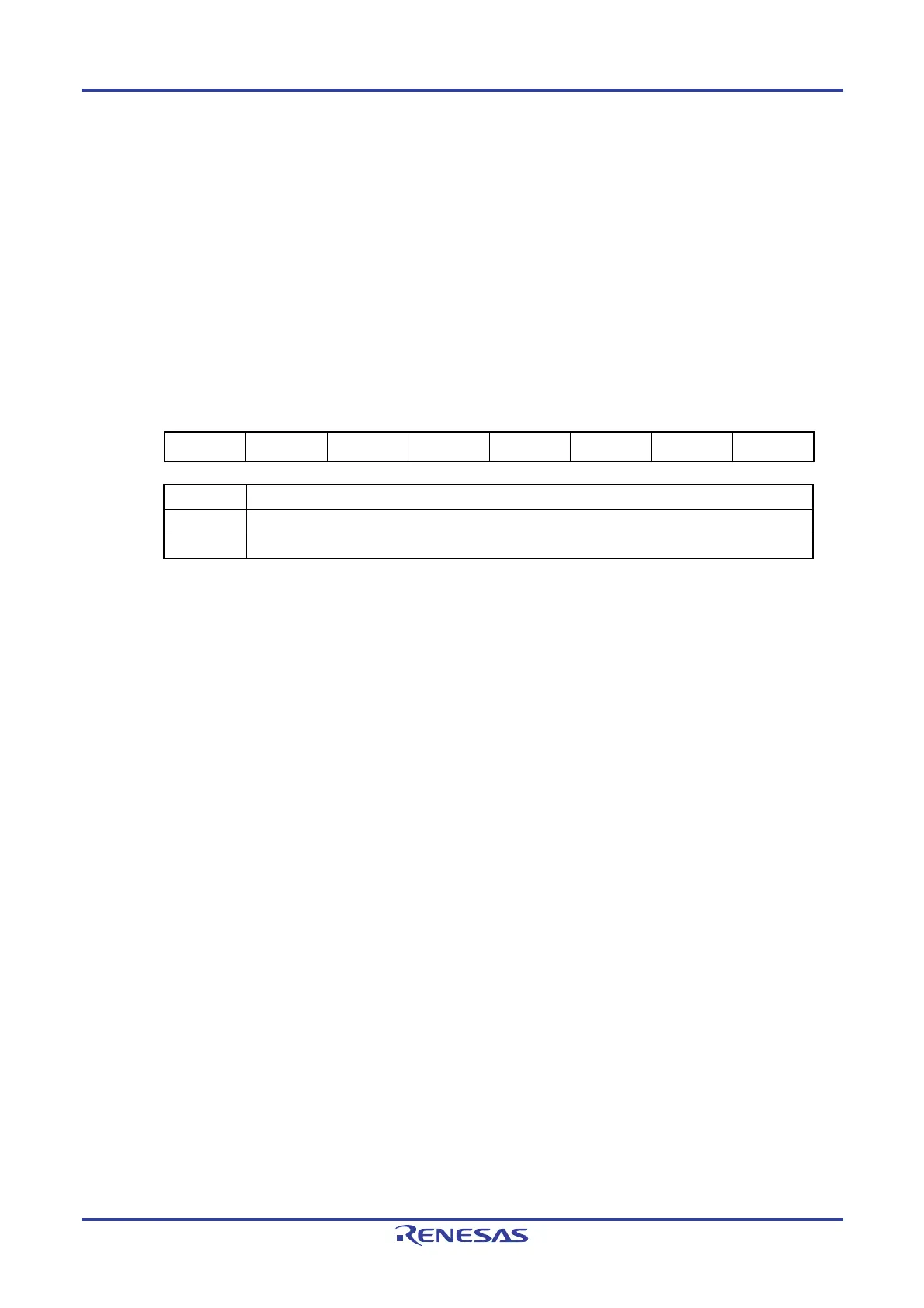
Figure 12-15. Format of Serial Clock Output Register 0 (CKO0)
Address: F0129H (CKO0) After reset: 03H R/W
Symbol
7 6 5 4 3 2 1 0
CKO0 0 0 0 0 0 0 CKO01
Note
CKO00
CKO0n Serial clock output of channel n
0 Serial clock output value is “0”.
1 Serial clock output value is “1”.
Note 16-pin products only.
Caution For 10-pin products, be sure to set bit 1 to 1 and clear bits 2 to 7 to 0.
For 16-pin products, be sure to clear bits 2 to 7 to 0.
Remark n: Channel number (n = 0, 1)

 Loading...


