RL78/G10 CHAPTER 10 A/D CONVERTER
R01UH0384EJ0311 Rev. 3.11 252
Dec 22, 2016
10.3.7 A/D test register (ADTES)
This register is used to select VSS as the analog input to be A/D converted. When the internal reference voltage (0.815
V (typ.)) is selected as the target of A/D conversion, the sampling capacitor must be discharged before A/D conversion of
this voltage proceeds.
The ADTES register can be set by an 8-bit memory manipulation instruction.
Reset signal generation sets this register to 00H.
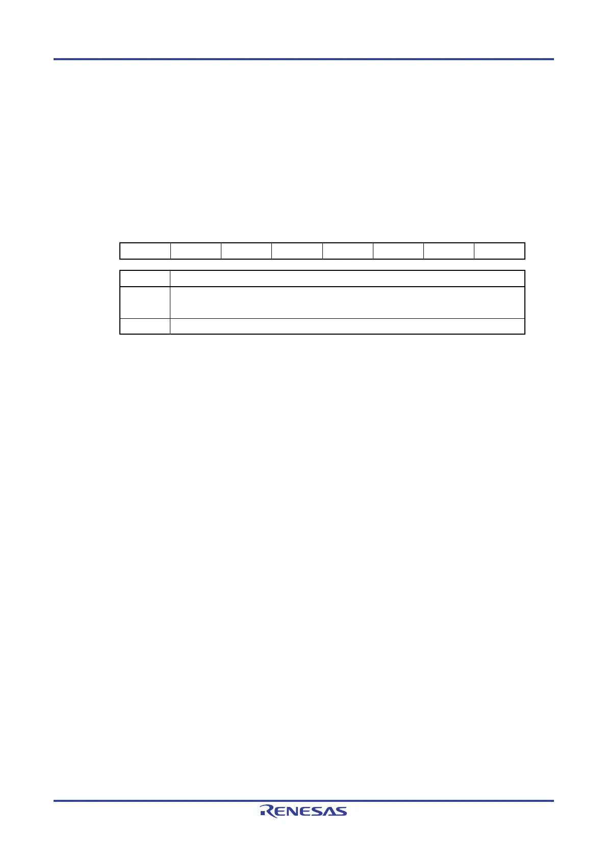
Figure 10-11. Format of A/D Test Register (ADTES)
Address: F0013H After reset: 00H R/W
Symbol 7 6 5 4 3 2 1 0
ADTES 0 0 0 0 0 0 ADTES1 0
ADTES1
Selection of target for A/D conversion
0
ANIx/internal reference voltage (0.815 V (typ.))
(This is specified using the analog input channel specification register (ADS).)
1 VSS (discharging the sampling capacitor)
Caution When A/D converting the internal reference voltage (0.815 V (typ.)), follow the procedure
described in 10.7.2 Setting up A/D conversion of the internal reference voltage (16-pin
products only), including discharge of the sampling capacitor once.
Remark Be sure to clear bits 0 and 2 to 7 to 0.
10.3.8 Registers controlling port function of analog input pins
Set up the registers for controlling the functions of the ports shared with the analog input pins of the A/D converter (port
mode register 0 (PM0) and port mode control register 0 (PMC0)). For details, see 4.3.1 Port mode registers 0, 4 (PM0,
PM4) and 4.3.5 Port mode control register 0 (PMC0).
For an example of settings when using a port pin for analog input of the A/D converter, see 4.5.3 Example of register
settings for port and alternate functions used.
When using the ANI0 to ANI6 pins for analog input of the A/D converter, set the bits in the port mode register 0 (PM0)
and port mode control register 0 (PMC0) corresponding to each port to 1.

 Loading...


