RL78/G10 CHAPTER 24 ELECTRICAL SPECIFICATIONS
R01UH0384EJ0311 Rev. 3.11 601
Dec 22, 2016
24.6 Analog Characteristics
24.6.1 A/D converter characteristics
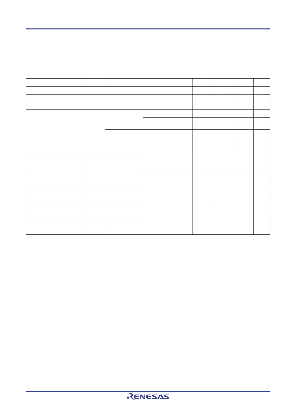
(Target pin: ANI0 to ANI6, internal reference voltage)
(T
A = −40 to +85°C, 2.4 V ≤ VDD ≤ 5.5 V, VSS = 0 V)
Parameter Symbol Conditions MIN. TYP. MAX. Unit
Resolution RES
8
10 bit
Overall error
Notes 1, 2, 3
AINL 10-bit resolution VDD = 5 V
±1.7 ±3.1
LSB
VDD = 3 V
±2.3 ±4.5
LSB
Conversion time tCONV
10-bit resolution
Target pin: ANI0
to ANI6
2.7 V ≤ VDD ≤ 5.5 V 3.4 18.4 µs
2.4 V ≤ VDD ≤ 5.5 V
Note 5
4.6 18.4 µs
10-bit resolution
Target pin:
internal reference
voltage
Note 6
2.4 V ≤ V
DD ≤ 5.5 V 4.6 18.4 µs
Zero-scale error
Notes 1, 2, 3, 4
EZS 10-bit resolution VDD = 5 V ±0.19 %FSR
VDD = 3 V ±0.39 %FSR
Full-scale error
Notes 1, 2, 3, 4
EFS 10-bit resolution VDD = 5 V ±0.29 %FSR
VDD = 3 V ±0.42 %FSR
Integral linearity error
Notes 1, 2, 3
ILE 10-bit resolution VDD = 5 V ±1.8 LSB
VDD = 3 V ±1.7 LSB
Differential linearity error
Notes 1, 2, 3
DLE 10-bit resolution V
DD = 5 V ±1.4 LSB
VDD = 3 V ±1.5 LSB
Analog input voltage VAIN Target pin: ANI0 to ANI6 0 VDD V
Target pin: internal reference voltage
Note 6
VREG
Note 7
V
Notes 1. TYP. Value is the average value at T
A = 25°C. MAX. value is the average value ±3σ at normal distribution.
2. These values are the results of characteristic evaluation and are not checked for shipment.
3. Excludes quantization error (±1/2 LSB).
4. This value is indicated as a ratio (%FSR) to the full-scale value.
5. Set the LV0 bit in the A/D converter mode register 0 (ADM0) to 0 when conversion is done in the operating
voltage range of 2.4 V ≤ V
DD < 2.7 V.
6. Set the LV0 bit in the A/D converter mode register 0 (ADM0) to 0 when the internal reference voltage is
selected as the target for conversion.
7. Refer to 24.6.3 Internal reference voltage characteristics.
Cautions 1. Arrange wiring and insert the capacitor so that no noise appears on the power supply/ground
line.
2. Do not allow any pulses that rapidly change such as digital signals to be input/output to/from the
pins adjacent to the conversion pin during A/D conversion.
3. Note that the internal reference voltage cannot be used as the reference voltage of the
comparator when the internal reference voltage is selected as the target for A/D conversion.

 Loading...


