RL78/G10 CHAPTER 12 SERIAL ARRAY UNIT
R01UH0384EJ0311 Rev. 3.11 301
Dec 22, 2016
12.3.16 Input switch control register (ISC)
The ISC1 and ISC0 bits in the ISC register are used to handle the combination of the external interrupt and the timer
array unit at the time of baud rate correction of UART0.
When bit 0 is set to 1, the input signal on the serial data input (RxD0) pin is input to the external interrupt input (INTP0),
making detection of the input edge signal of the start bit in the form of the INTP0 interrupt possible.
When bit 1 is set to 1, the input signal on the serial data input (RxD0) pin is input to the timer input pin (TI01). The width
at the baud rate (transfer rate) of the other party can be measured by using the timer array unit input pulse interval
measurement mode with the input edge signal of the start bit as a trigger.
The ISC register can be set by a 1-bit or 8-bit memory manipulation instruction.
Reset signal generation clears the ISC register to 00H.
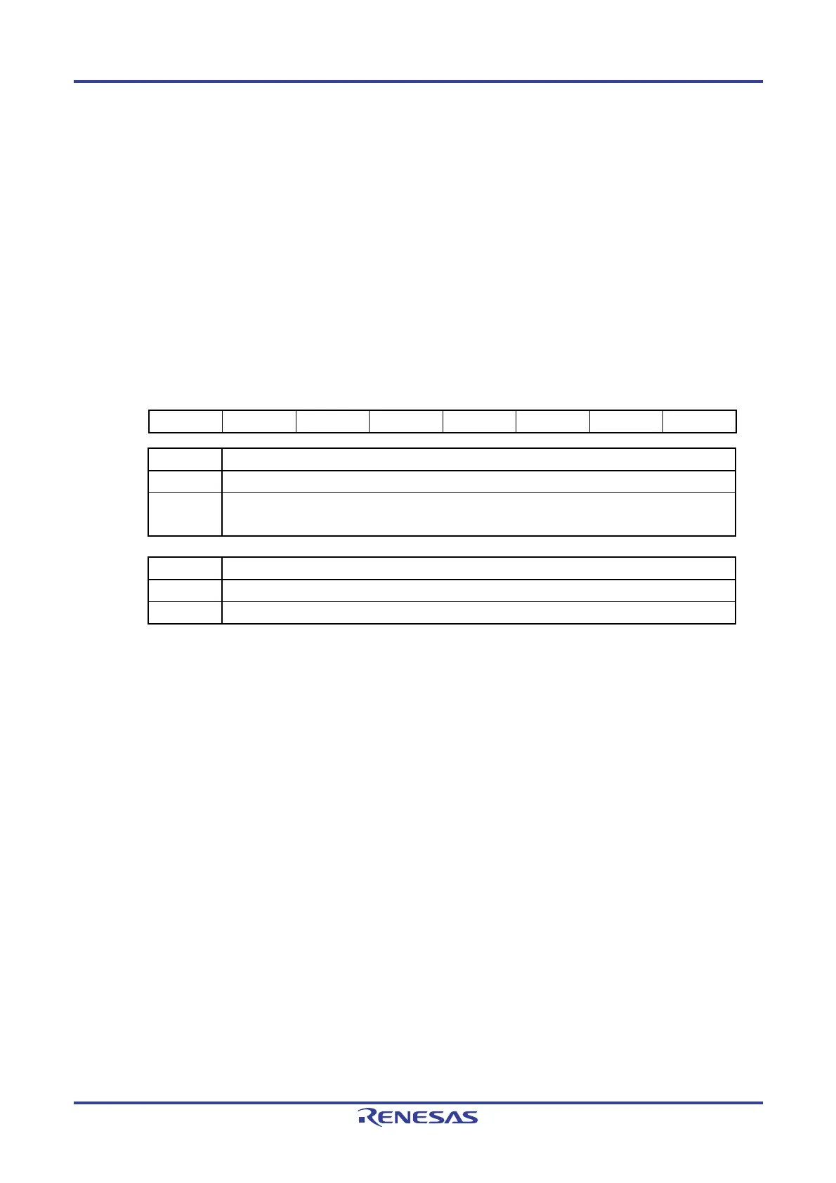
Figure 12-19. Format of Input Switch Control Register (ISC)
Address: F00730H After reset: 00H R/W
Symbol 7 6 5 4 3 2 1 0
ISC 0 0 0 0 0 0 ISC1 ISC0
ISC1 Switching the channel 1 of the timer array unit
0 Select the input signal on TI01 pin as the timer input (normal operation)
1 Select the input signal on RxD0 pin as the timer input
(Detection of the wake-up signal and pulse-width-measurement for baud rate correction)
ISC0 Switching the external interrupt (INTP0)
0 Select the input signal on INTP0 pin as the external interrupt input (normal operation)
1 Select the input signal on RxD0 pin as the external interrupt input (detection of the wake-up signal)
Caution Be sure to clear bits 2 to 7 to 0.

 Loading...


