RL78/G10 CHAPTER 1 OUTLINE
R01UH0384EJ0311 4
Dec 22, 2016
Note For the fields of application, refer to Figure 1-1 Part Number, Memory Size, and Package of RL78/G10.
Caution The part number represents the number at the time of publication.
Be sure to review the latest part number through the target product page in the Renesas Electronics
Corp.website.
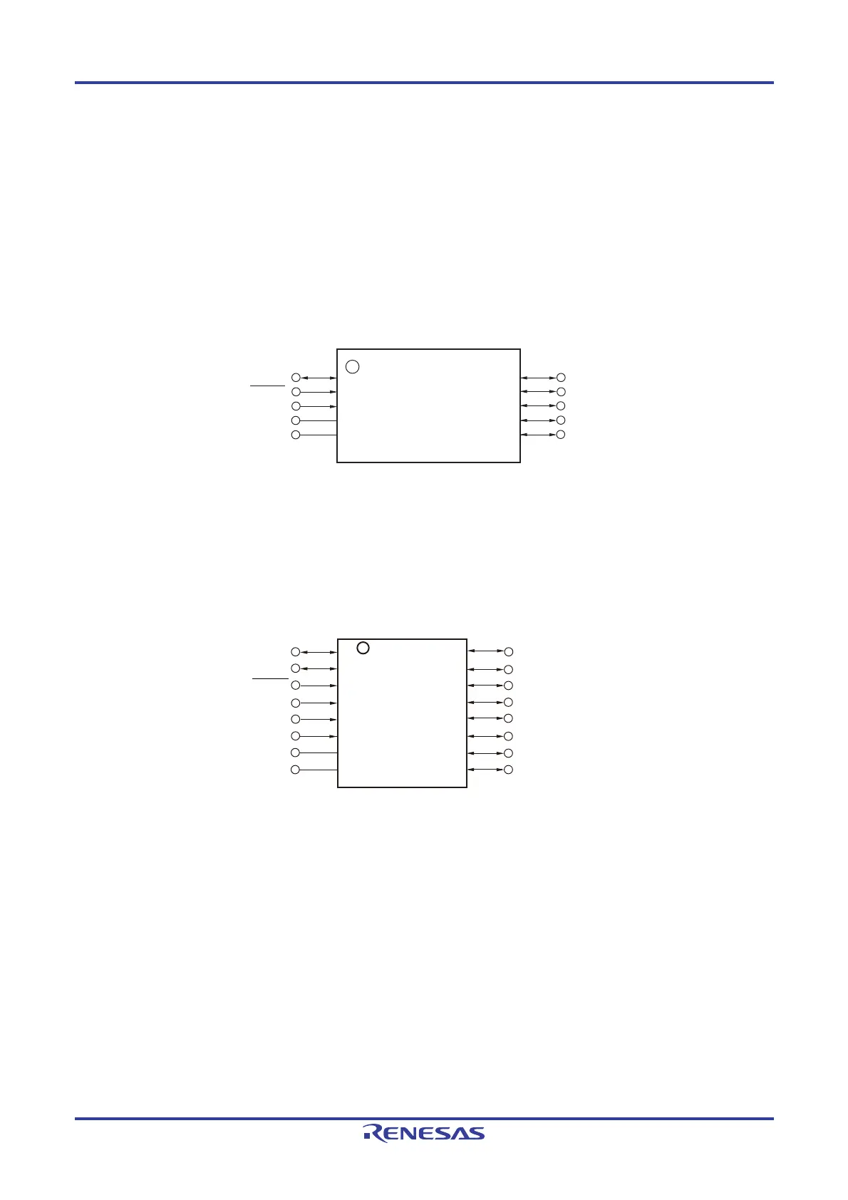
1.3 Pin Configuration (Top View)
1.3.1 10-pin products
• 10-pin plastic LSSOP (4.4 × 3.6 mm, 0.65 mm pitch)
10
9
8
7
6
1
2
3
4
5
P04/ANI3/TI01/TO01/KR5
P03/ANI2/TO00/KR4/(INTP1)
P02/ANI1/SCK00/SCL00/PCLBUZ0/KR3
P01/ANI0/SI00/RXD0/SDA00/KR2
P00/SO00/TXD0/INTP1
P40/KR0/TOOL0/(PCLBUZ0)/(TI01/TO01)
P125/KR1/RESET
P137/TI00/INTP0
V
SS
VDD
RL78/G10
(Top View)
Remarks 1. For pin identification, see 1.4 Pin Identification.
2. Functions in parentheses in the above figure can be assigned via settings in the peripheral I/O redirection
register (PIOR). See Figure 4-6 Format of Peripheral I/O Redirection Register (PIOR).
1.3.2 16-pin products
• 16-pin plastic SSOP (4.4 × 5.0 mm, 0.65 mm pitch)
1
2
3
4
5
P41/TI03/INTP2
P40/KR0/TOOL0/(PCLBUZ0)/(TI01/TO01)
P125/KR1/RESET
P137/TI00/INTP0
P122/X2/EXCLK/(INTP2)
P121/X1/(INTP3)
V
SS
V
DD
6
7
8
16
15
14
13
12
11
10
9
P07/SDAA0/TO03/ANI6/SCK01
P06/SCLA0/INTP3/ANI5/SI01
P05/ANI4/TI02/TO02/SO01
P04/ANI3/TI01/TO01/KR5/IVREF0
P03/ANI2/TO00/KR4/(INTP1)/IVCMP0
P02/ANI1/SCK00/SCL00/PCLBUZ0/KR3/
P01/ANI0/SI00/RXD0/SDA00/KR2
P00/SO00/TXD0/INTP1
VCOUT0
RL78/G10
(Top View)
Remarks 1. For pin identification, see 1.4 Pin Identification.
2. Functions in parentheses in the above figure can be assigned via settings in the peripheral I/O redirection
register (PIOR). See Figure 4-6 Format of Peripheral I/O Redirection Register (PIOR).

 Loading...


