RL78/G10 CHAPTER 24 ELECTRICAL SPECIFICATIONS
R01UH0384EJ0311 Rev. 3.11 602
Dec 22, 2016
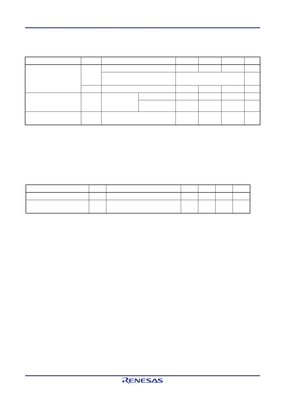
24.6.2 Comparator characteristics
(TA = −40 to +85°C, 2.0 V ≤ VDD ≤ 5.5 V, VSS = 0 V)
Parameter Symbol Conditions MIN. TYP. MAX. Unit
Input voltage range IVREF IVREF0 pin input (when C0VFR bit = 0)
0
VDD - 1.4 V
Internal reference voltage (when C0VRF
bit = 1)
Note 1
V
REG
Note 2
V
IVCMP IVCMP0 pin input
-0.3
VDD + 0.3 V
Output delay td
V
DD = 3.0 V,
input slew rate > 50
mV/µs
High-speed mode
0.5 µs
Low-speed mode
2.0 µs
Operation stabilization wait
time
t
CMP
100
µs
Notes 1. When the internal reference voltage is selected as the reference voltage of the comparator, the internal
reference voltage cannot be used as the target for A/D conversion.
2. Refer to 24.6.3 Internal reference voltage characteristics.
24.6.3 Internal reference voltage characteristics
(TA = −40 to +85°C, 2.0 V ≤ VDD ≤ 5.5 V, VSS = 0 V)
Parameter Symbol Conditions MIN. TYP. MAX. Unit
Internal reference voltage VREG 0.74 0.815 0.89 V
Operation stabilization wait time tAMP
When A/D converter is used
(ADS register = 07H)
5 µs
Note The internal reference voltage cannot be simultaneously used by the A/D converter and the comparator; only one
of them must be selected.

 Loading...


