RL78/G10 CHAPTER 1 OUTLINE
R01UH0384EJ0311 8
Dec 22, 2016
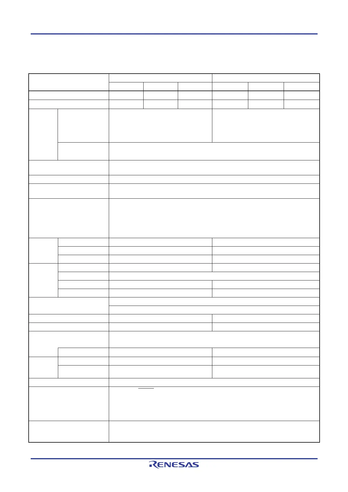
1.6 Outline of Functions
This outline describes the function at the time when Peripheral I/O redirection register (PIOR) is set to 00H.
Item 10-pin 16-pin
R5F10Y14 R5F10Y16 R5F10Y17 R5F10Y44 R5F10Y46 R5F10Y47
Code flash memory 1 KB 2 KB 4 KB 1 KB 2 KB 4 KB
RAM 128 B 256 B 512 B 128 B 256 B 512 B
Main
system
clock
High-speed system
clock
—
X1, X2 (crystal/ceramic) oscillation, external
main system clock input (EXCLK):
1 to 20 MHz: V
DD = 2.7 to 5.5 V
1 to 5 MHz: V
DD = 2.0 to 5.5 V
Note 3
High-speed on-chip
oscillator clock
• 1.25 to 20 MHz (V
DD = 2.7 to 5.5 V)
• 1.25 to 5 MHz (V
DD = 2.0 to 5.5 V
Note 3
)
Low-speed on-chip oscillator
clock
15 kHz (TYP)
General-purpose register 8-bit register × 8
Minimum instruction execution
time
0.05 μs (20 MHz operation)
Instruction set • Data transfer (8 bits)
• Adder and subtractor/logical operation (8 bits)
• Multiplication (8 bits × 8 bits)
• Rotate, barrel shift, and bit manipulation
(set, reset, test, and Boolean operation), etc.
I/O port Total 8 14
CMOS I/O 6 (N-ch open-drain output (VDD tolerance): 2) 10 (N-ch open-drain output (VDD tolerance): 4)
CMOS input 2 4
Timer 16-bit timer 2 channels 4 channels
Watchdog timer 1 channel
12-bit interval timer — 1 channel
Timer output 2 channels (PWM output: 1) 4 channels (PWM outputs: 3
Note 1
)
Clock output/buzzer output 1
2.44 kHz to 10 MHz: (Peripheral hardware clock: fMAIN = 20 MHz operation)
Comparator — 1
8-/10-bit resolution A/D converter 4 channels 7 channels
Serial interface [10-pin products] CSI: 1 channel/simplified I
2
C: 1 channel/UART: 1 channel
[16-pin products] CSI: 2 channels/simplified I
2
C: 1 channel/UART: 1 channel
I
2
C bus — 1 channel
Vectored
interrupt
sources
Internal 8 14
External 3 5
Key interrupt 6
Reset • Reset by RESET pin
• Internal reset by watchdog timer
• Internal reset by selectable power-on-reset
• Internal reset by illegal instruction execution
Note 2
• Internal reset by data retention lower limit voltage
Selectable power-on-reset circuit • Detection voltage
Rising edge (V
SPOR): 2.25 V/2.68 V/3.02 V/4.45 V (max.)
Falling edge (V
SPDR): 2.20 V/2.62 V/2.96 V/4.37 V (max.)

 Loading...


