RL78/G10 CHAPTER 12 SERIAL ARRAY UNIT
R01UH0384EJ0311 Rev. 3.11 285
Dec 22, 2016
12.3.3 Serial mode register 0n (SMR0nH, SMR0nL)
The SMR0nH and SMR0nL registers are registers that set an operation mode of channel n. It is also used to select an
operation clock (fMCK), specify whether the serial clock (fSCK) may be input or not, set a start trigger, an operation mode
(CSI, UART, or I
2
C), and an interrupt source. This register is also used to invert the level of the receive data only in the
UART mode.
Rewriting the SMR0nH and SMR0nL registers is prohibited when the operation is enabled (when SE0n = 1). However,
the MD0n0 bit can be rewritten even when the operation is enabled.
The SMR0nH and SMR0nL registers can be set by an 8-bit memory manipulation instruction.
Reset signal generation sets the SMR0nH and SMR0nL registers to 00H and 20H, respectively.
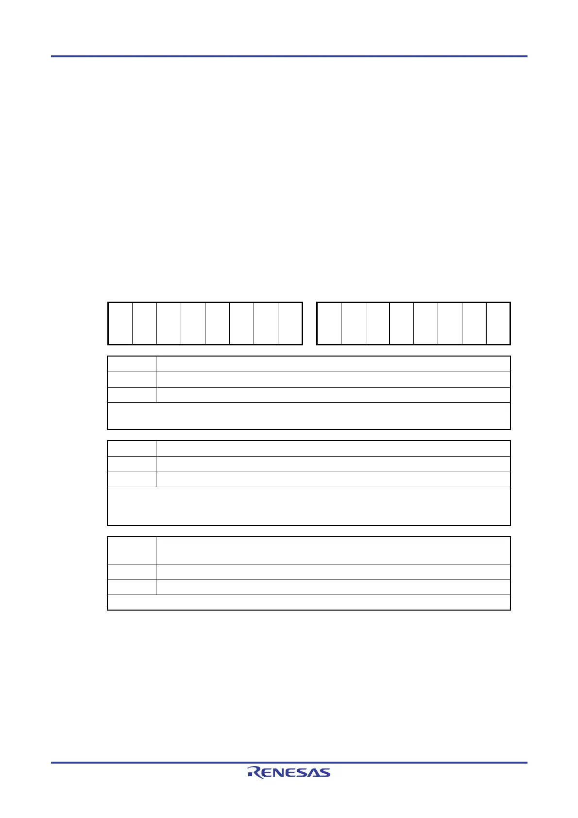
Figure 12-5. Format of Serial Mode Register 0n (SMR0nH, SMR0nL) (1/2)
Address: F0111H (SMR00H), F0113H (SMR01H) Address: F0110H (SMR00L), F0112H (SMR01L)
After reset: 00H R/W After reset: 20H R/W
Symbol: SMR0nH Symbol: SMR0nL
15 14 13 12 11 10 9 8 7 6 5 4 3 2 1 0
CKS
0n
CCS
0n
0 0 0 0 0 STS
0n
Note 1
0 SIS
0n0
Note 2
10 0 MD
0n2
MD
0n1
MD
0n0
CKS0n Selection of operation clock (fMCK) of channel n
0 Operation clock CK00 set by the SPS0 register
1 Operation clock CK01 set by the SPS0 register
Operation clock (fMCK) is used by the edge detector. In addition, depending on the setting of the CCS0n bit and the
SDR0nH register, a transfer clock (f
TCLK) is generated.
CCS0n Selection of transfer clock (fTCLK) of channel n
0 Divided operation clock fMCK specified by the CKS0n bit
1 Clock input fSCK from the SCKp pin (slave transfer in CSI mode)
Transfer clock fTCLK is used for the shift register, communication controller, output controller, interrupt controller,
and error controller. When CCS0n = 0, the division ratio of operation clock (f
MCK) is set by the higher 7 bits of the
SDR0nH register.
STS0n
Note 1
Selection of start trigger source
0 Only software trigger is valid (selected for CSI, UART transmission, and simplified I
2
C).
1 Valid edge of the RXD0 pin (selected for UART reception)
Transfer is started when the above source is satisfied after 1 is set to the SS0 register.
Notes 1. Provided in the SMR01H register only.
2. Provided in the SMR01L register only.
Caution Do not change the initial values of the following bits.
SMR00H: Be sure to clear bits 0 to 5 to 0.
SMR01H: Be sure to clear bits 1 to 5 to 0.
SMR00L: Be sure to clear bits 3, 4, 6, and 7 to 0, and set bit 5 to 1.
SMR01L: Be sure to clear bits 3, 4, and 7 to 0, and set bit 5 to 1.
Remark n: Channel number (n = 0, 1)

 Loading...


