RL78/G10 CHAPTER 13 SERIAL INTERFACE IICA
R01UH0384EJ0311 Rev. 3.11 428
Dec 22, 2016
13.4 I
2
C Bus Mode Functions
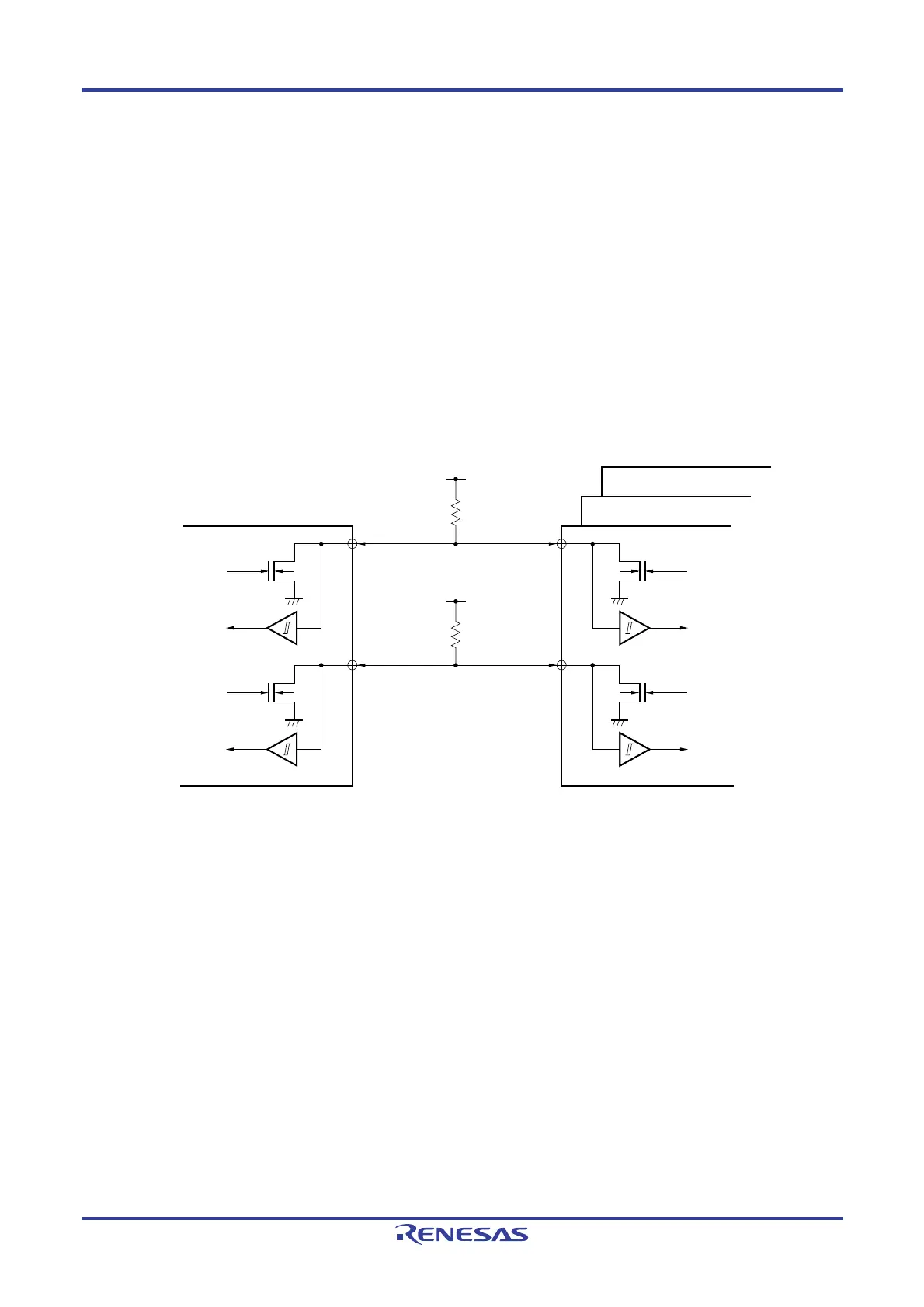
13.4.1 Pin configuration
The serial clock pin (SCLA0) and the serial data bus pin (SDAA0) are configured as follows.
(1) SCLA0 .... This pin is used for serial clock input and output.
This pin is an N-ch open-drain output for both master and slave devices. Input is Schmitt input.
(2) SDAA0 .... This pin is used for serial data input and output.
This pin is an N-ch open-drain output for both master and slave devices. Input is Schmitt input.
Since outputs from the serial clock line and the serial data bus line are N-ch open-drain outputs, an external pull-up
resistor is required.
Figure 13-12. Pin Configuration Diagram
Master device
Clock output
(Clock input)
Data output
Data input
V
SS
V
SS
SCLA0
SDAA0
V
DD
V
DD
(Clock output)
Clock input
Data output
Data input
V
SS
V
SS
Slave device
SCLA0
SDAA0

 Loading...


