RL78/G10 CHAPTER 24 ELECTRICAL SPECIFICATIONS
R01UH0384EJ0311 Rev. 3.11 593
Dec 22, 2016
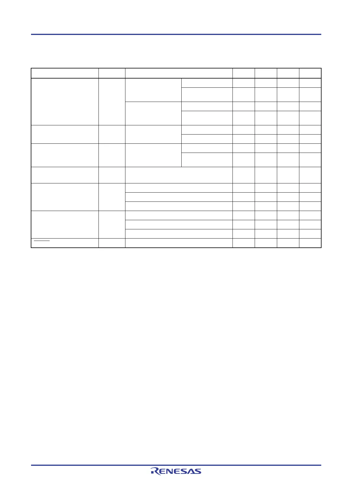
24.4 AC Characteristics
(TA = −40 to +85°C, 2.0 V ≤ VDD ≤ 5.5 V, VSS = 0 V)
Items Symbol Conditions
MIN. TYP. MAX. Unit
Instruction cycle (minimum
instruction execution time)
T
CY
When high-speed on-
chip oscillator clock (f
IH)
is selected
2.7 V ≤ V
DD ≤ 5.5 V 0.05 0.8 µs
2.0 V ≤ VDD < 2.7 V 0.2 0.8 µs
When high-speed
system clock (f
MX) is
selected
2.7 V ≤ V
DD ≤ 5.5 V 0.05 1.0 µs
2.0 V ≤ VDD < 2.7 V 0.2 1.0 µs
External system clock
frequency
T
EX 2.7 V ≤ VDD ≤ 5.5 V 1.0 20 MHz
2.0 V ≤ VDD < 2.7 V 1.0 5 MHz
External system clock input
high-level width, low-level
width
T
EXH, TEXL 2.7 V ≤ VDD ≤ 5.5 V 24 ns
2.0 V ≤ VDD < 2.7 V 95 ns
TI00 to TI03 input high-level
width, low-level width
t
TIH, tTIL Noise filter is not used
1/f
MCK +
10
ns
TO00 to TO03 output
frequency
f
TO 4.0 V ≤ VDD ≤ 5.5 V
10 MHz
2.7 V ≤ VDD < 4.0 V
5 MHz
2.0 V ≤ VDD < 2.7 V
2.5 MHz
PCLBUZ0 output frequency fPCL 4.0 V ≤ VDD ≤ 5.5 V
10 MHz
2.7 V ≤ VDD < 4.0 V
5 MHz
2.0 V ≤ VDD < 2.7 V
2.5 MHz
RESET low-level width tRSL 10 µs
Remark fMCK: Timer array unit operation clock frequency
(Operation clock to be set by the timer clock select register 0 (TPS0) and the CKS0n1 bit of timer mode register
0nH (TMR0nH). n: Channel number (n = 0 to 3))

 Loading...


