RL78/G10 CHAPTER 12 SERIAL ARRAY UNIT
R01UH0384EJ0311 Rev. 3.11 326
Dec 22, 2016
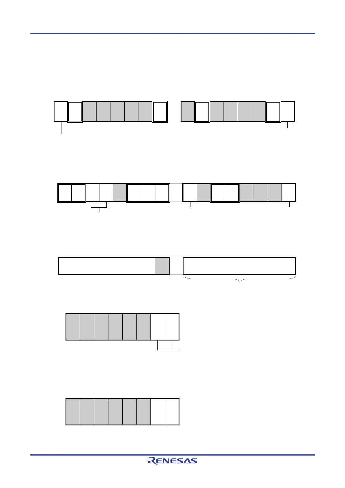
(1) Register setting
Figure 12-38. Example of Contents of Registers for Master Transmission/Reception of 3-Wire Serial I/O
(CSI00, CSI01
Note
) (1/2)
(a) Serial mode register 0n (SMR0nH, SMR0nL)
Symbol:SMR0nH Symbol:SMR0nL
15 14 13 12 11 10 9 8 7 6 5 4 3 2 1 0
CKS0n
0/1
CCS0n
0
0
0
0
0
0
STS0n
0
0
SIS0n0
0
1
0
0
0
MD0n1
0
MD0n0
0/1
Interrupt source of channel n
0: Transfer end interrupt
1: Buffer empty interrupt
Operation clock (fMCK) of channel n
0: Prescaler output clock CK00 set by the SPS0 register
1: Prescaler output clock CK01 set by the SPS0 register
(b) Serial communication operation setting register 0n (SCR0nH, SCR0nL)
Symbol:SCR0nH Symbol:SCR0nL
15 14 13 12 11 10 9 8
7 6 5 4 3 2 1 0
TXE0n
1
RXE0n
1
DAP0n
0/1
CKP0n
0/1
0
EOC0n
0
PTC0n1
0
PTC0n0
0
DIR0n
0/1
0
SLC0n1
0
SLC0n0
0
0
1
1
DLS0n0
0/1
Selection of data transfer sequence
0: Inputs/outputs data with MSB first
1: Inputs/outputs data with LSB first.
Setting of data length
0: 7-bit data length
1: 8-bit data length
Selection of the data and clock
phase (For details about the setting,
see 12.3 Registers Controlling
Serial Array Unit.)
(c) Serial data register 0n (SDR0nH, SDR0nL)
15 14 13 12 11 10 9 8
7 6 5 4 3 2 1 0
Baud rate setting
(Operation clock (f
MCK) division setting)
0
Transmit data setting/receive data register
(d) Serial clock output register 0 (CKO0) … Sets only the bits of the target channel.
(e) Serial output register 0 (SO0) … Sets only the bits of the target channel.
(Note and Remarks are listed on the next page.)
Symbol: 7 6 5 4 3 2 1 0
CKO0
0
0
0
0
0
0
CKO01
Note
0/1
CKO00
0/1
Communication starts when these bits are 1 if the clock
phase is non-inversion (the CKP0n bit of the SCR0n = 0).
If the clock phase is inverted (CKP0n = 1), communication
starts when these bits are 0.
Symbol: 7 6 5 4 3 2 1 0
SO0
0
0
0
0
0
0
SO01
Note
0/1
SO00
0/1
SIOp

 Loading...


