RL78/G10 CHAPTER 6 TIMER ARRAY UNIT
R01UH0384EJ0311 Rev. 3.11 140
Dec 22, 2016
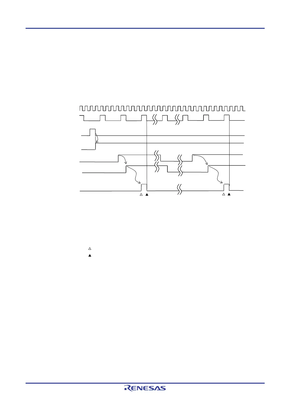
(2) When valid edge of input signal via the TI0n pin is selected (CCS0n = 1)
The count clock (f
TCLK) is the signal that detects valid edge of input signal via the TI0n pin and synchronizes next
rising f
MCK. The count clock (fTCLK) is delayed for 1 to 2 period of fMCK from the input signal via the TI0n pin (when a
noise filter is used, it is delayed for 3 to 4 clock cycles).
Counting of timer count register 0n (TCR0n) delayed by one f
CLK cycle period from rising edge of the count clock
(f
TCLK), because of synchronization with fCLK. But, this is described as “counting at valid edge of input signal via the
TI0n pin”, as a matter of convenience.
Figure 6-23. Timing of fCLK and Count Clock (fTCLK) (When CCS0n = 1, noise filter unused)
<1> Setting TS0n bit to 1 enables the timer to be started and the operation enters wait state for valid edge of
input signal via the TI0n pin.
<2> The rise of input signal via the TI0n pin is sampled by f
MCK.
<3> The edge is detected by the rising of the sampled signal and the detection signal (count clock (f
TCLK)) is
output.
Remarks 1. : Rising edge of the count clock (f
TCLK
)
: Synchronization, increment/decrement of counter
2. f
CLK: CPU/peripheral hardware clock
f
MCK: Operation clock of channel n
3. The waveform of the input signal via TI0n pin of the input pulse interval measurement, the
measurement of high/low width of input signal, and the delay counter, the one-shot pulse
output are the same as that shown in Figure 6-23.
fMC
TS0n (Write)
TE0n
TI0n input
<1>
<2>
Rising edge
detection signal (f
TCLK)
Sampling wave
Edge detection
Edge detection
<3>
fCL

 Loading...


