RL78/G10 CHAPTER 6 TIMER ARRAY UNIT
R01UH0384EJ0311 Rev. 3.11 215
Dec 22, 2016
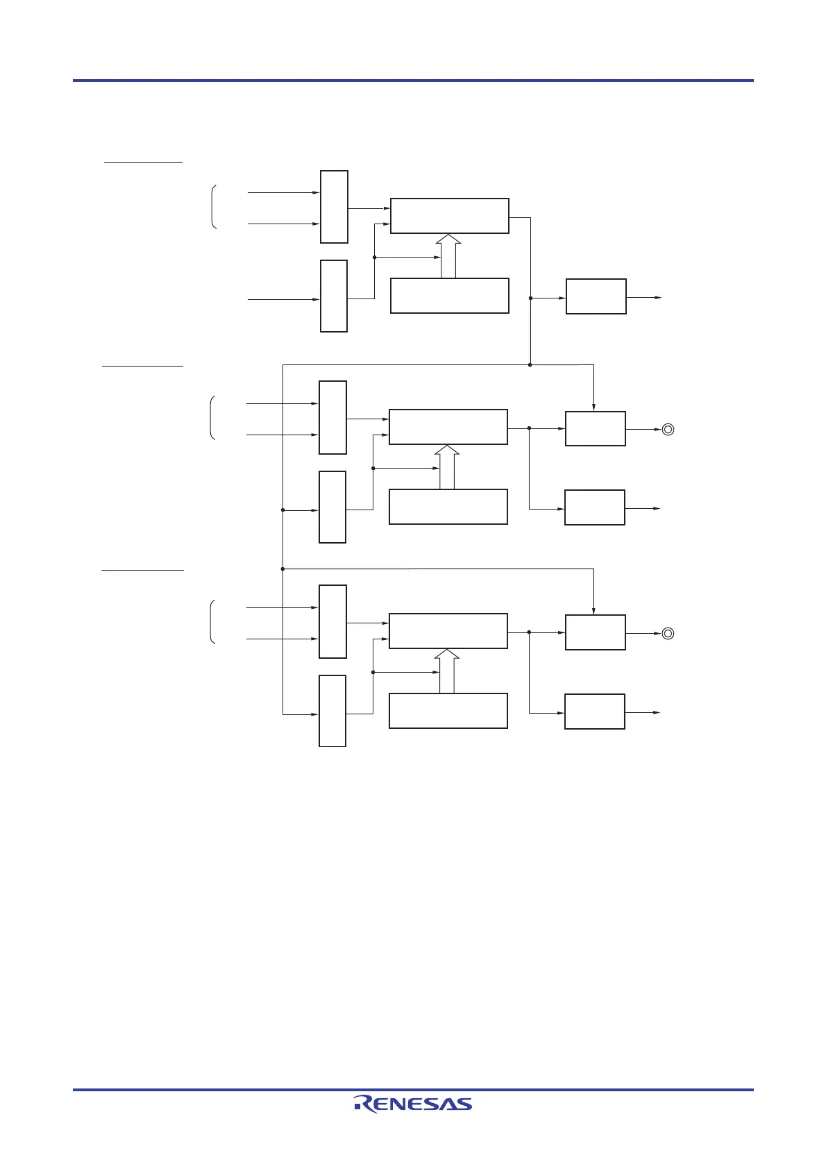
Figure 6-79. Block Diagram of Operation as Multiple PWM Output Function (Output Two Types of PWMs)
Interrupt signal
(INTTM0n)
Interrupt
controller
Clock selection
Trigger selection
Operation clock
CK00
CK01
TS0n
Interrupt signal
(INTTM0p)
Interrupt
controller
Clock selection
Trigger selection
Operation clock
CK00
CK01
TO0p pin
Output
controller
Master channel
(interval timer mode)
Slave channel 1
(one-count mode)
Interrupt signal
(INTTM0q)
Interrupt
controller
Clock selection
Trigger selection
Operation clock
CK00
CK01
TO0q pin
Output
controller
Slave channel 2
(one-count mode)
Timer counter
register 0n (TCR0n)
Timer data
register 0n (TDR0n)
Timer counter
register 0p (TCR0p)
Timer data
register 0p (TDR0p)
Timer counter
register 0q (TCR0q)
Timer data
register 0q (TDR0q)
Remark n: Channel number (n = 0)
p: Channel number of slave channel 1, q: Channel number of slave channel 2
n < p < q ≤ 3 (Where p and q are consecutive integers greater than n)

 Loading...


