RL78/G10 CHAPTER 10 A/D CONVERTER
R01UH0384EJ0311 Rev. 3.11 241
Dec 22, 2016
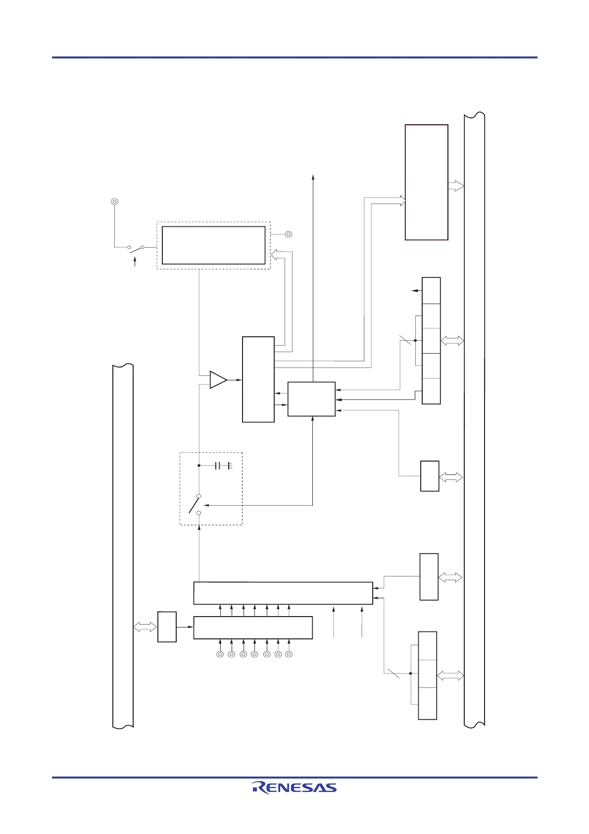
Figure 10-1. Block Diagram of A/D Converter
Selector
Sample & hold circuit
Analog input channel
specification register (ADS)
A/D conversion result higher/
lower-order bit storage register
(ADCRH, ADCRL)
A/D voltage comparator
Controller
Comparison
voltage
generator
VDD
VSS
ADCE bit
A/D converter mode
register 0 (ADM0)
A/D converter mode
register 2 (ADM2)
Successive
approximation register
(SAR)
ADCS
FR1
ADCEFR0
V
SS
3
ANI0
ANI1
ANI2
ANI3
LV0
3
ADS1
ADS2
ADS0
ADTYP
ANI4
ANI5
ANI6
A/D test register
(ADTES)
Internal reference
voltage
(0.815 V (typ.))
ADTES1
Note 2
Note 2
Note 2
Note 1
Note 2
Digital port control
INTAD
PMC0
Port mode control register 0 (PMC0)
V
SS
Internal bus
Internal bus
Notes 1. For 10-pin products, ANI0 to ANI3.
2. 16-pin products only.

 Loading...


