RL78/G10 CHAPTER 12 SERIAL ARRAY UNIT
R01UH0384EJ0311 Rev. 3.11 346
Dec 22, 2016
(1) Register setting
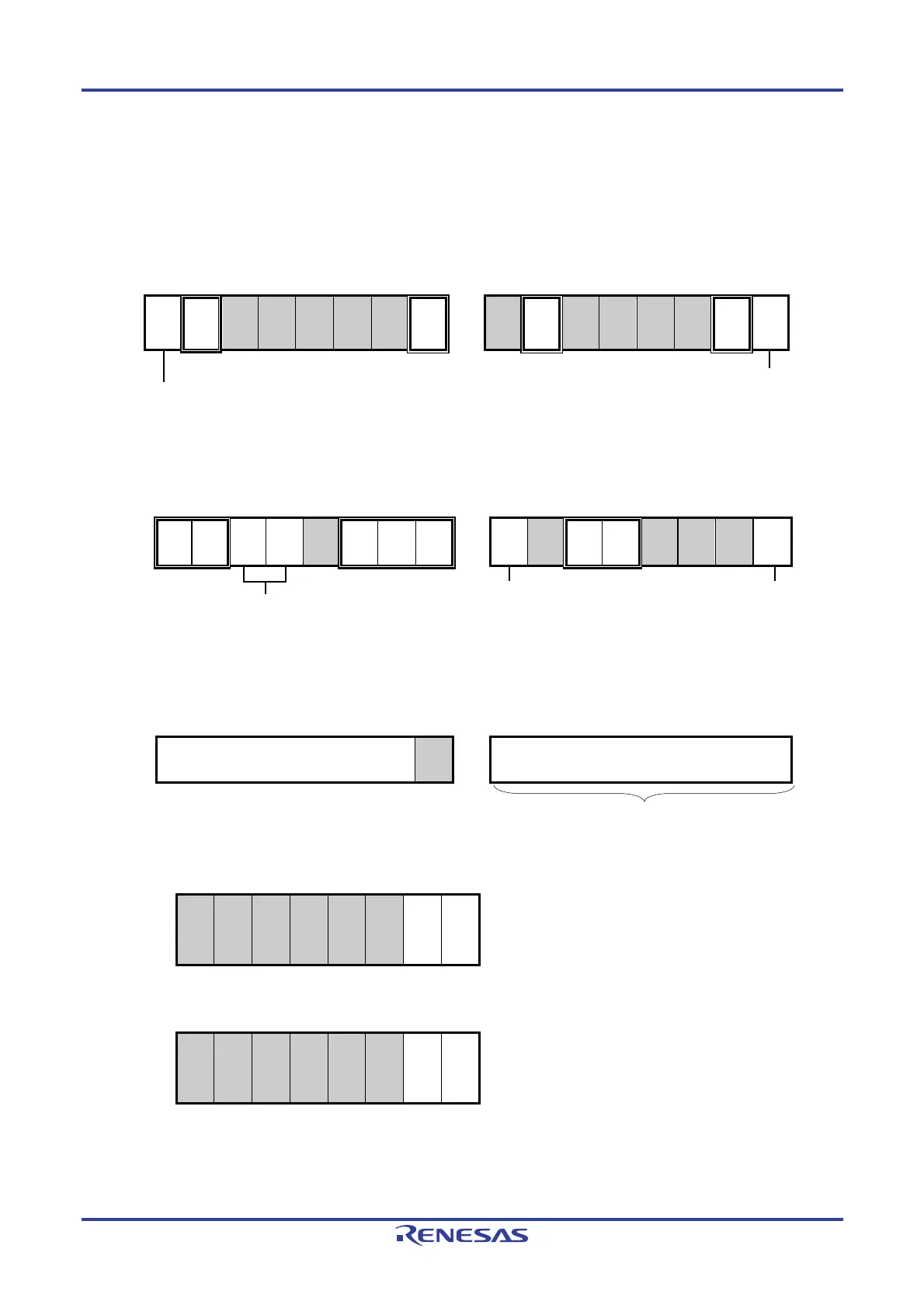
Figure 12-54. Example of Contents of Registers for Slave Reception of 3-Wire Serial I/O
(CSI00, CSI01
Note
) (1/2)
(a) Serial mode register 0n (SMR0nH, SMR0nL)
Symbol:SMR0nH Symbol:SMR0nL
15 14 13 12 11 10 9 8 7 6 5 4 3 2 1 0
CKS0n
0/1
CCS0n
0
0
0
0
0
0
STS0n
0
0
SIS0n0
0
1
0
0
0
MD0n1
0
MD0n0
0/1
Interrupt source of channel n
0: Transfer end interrupt
Operation clock (fMCK) of channel n
0: Prescaler output clock CK00 set by the SPS0 register
1: Prescaler output clock CK01 set by the SPS0 register
(b) Serial communication operation setting register 0n (SCR0nH, SCR0nL)
Symbol: SCR0nH Symbol: SCR0nL
15 14 13 12 11 10 9 8 7 6 5 4 3 2 1
TXE0n
0
RXE0n
1
DAP0n
0/1
CKP0n
0/1
0
EOC0n
0
PTC0n1
0
PTC0n0
0
DIR0n
0/1
0
SLC0n1
0
SLC0n0
0
0
1
1
DLS0n0
0/1
Selection of data transfer sequence
0: Inputs/outputs data with MSB first
1: Inputs/outputs data with LSB first.
Setting of data length
0: 7-bit data length
1: 8-bit data length
Selection of the data and clock
phase (For details about the setting,
see 12.3 Registers Controlling
Serial Array Unit.)
(c) Serial data register 0n (SDR0nH, SDR0nL)
Symbol: SDR0nH Symbol: SDR0nL
15 14 13 12 11 10 9 8 7 6 5 4 3 2 1 0
0000000
Baud rate setting
0
Receive data
(d) Serial clock output register 0 (CKO0) … The Register that not used in this mode.
(e) Serial output register 0 (SO0) …The Register that not used in this mode.
(Note and Remarks are listed on the next page.)
Symbol: 7 6 5 4 3 2 1 0
CKO0
0
0
0
0
0
0
CKO01
Note
×
CKO00
×
Symbol: 7 6 5 4 3 2 1 0
SO0
0
0
0
0
0
0
SO01
Note
×
SO00
×
SIOp

 Loading...


