RL78/G10 CHAPTER 3 CPU ARCHITECTURE
R01UH0384EJ0311 Rev. 3.11 25
Dec 22, 2016
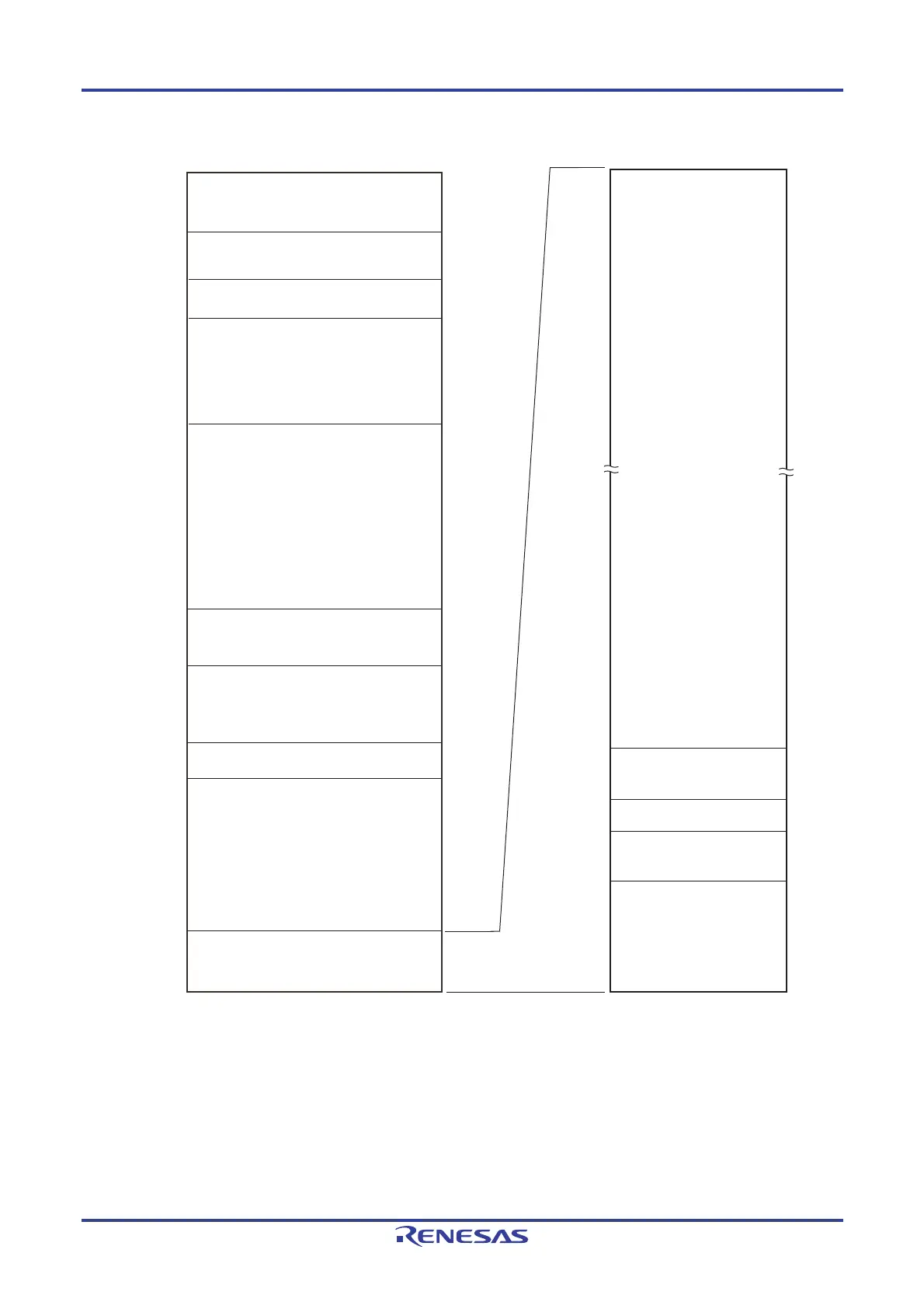
Figure 3-2. Memory Map for the R5F10Y16 and R5F10Y46
Program area
CALLT table area
64 bytes
Vector table area
128 bytes
Option byte area
4 bytes
Note
On-chip debug
security ID setting area
10 bytes
Note
FFFFFH
FFF00H
FFEFFH
FFEF8H
FFEF7H
00000H
007FFH
FFDE0H
FFDDFH
Reserved
Reserved
Special function register (2nd SFR)
2KB
Reserved
Mirror
2KB
Reserved
FFEE0H
FFEDFH
F0000H
EFFFFH
F0800H
F07FFH
F8000H
F7FFFH
F8800H
F87FFH
007FFH
000CEH
000CDH
000C4H
000C3H
000C0H
000BFH
00080H
0007FH
00000H
Special function register (SFR)
256 bytes
General-purpose
register 8 bytes
RAM
256 bytes
Code flash memory
2KB
Note Set the option bytes to 000C0H to 000C3H, and the on-chip debug security IDs to 000C4H to 000CDH.
Caution Access to the reserved area is prohibited.

 Loading...


