RL78/G10 CHAPTER 24 ELECTRICAL SPECIFICATIONS
R01UH0384EJ0311 Rev. 3.11 589
Dec 22, 2016
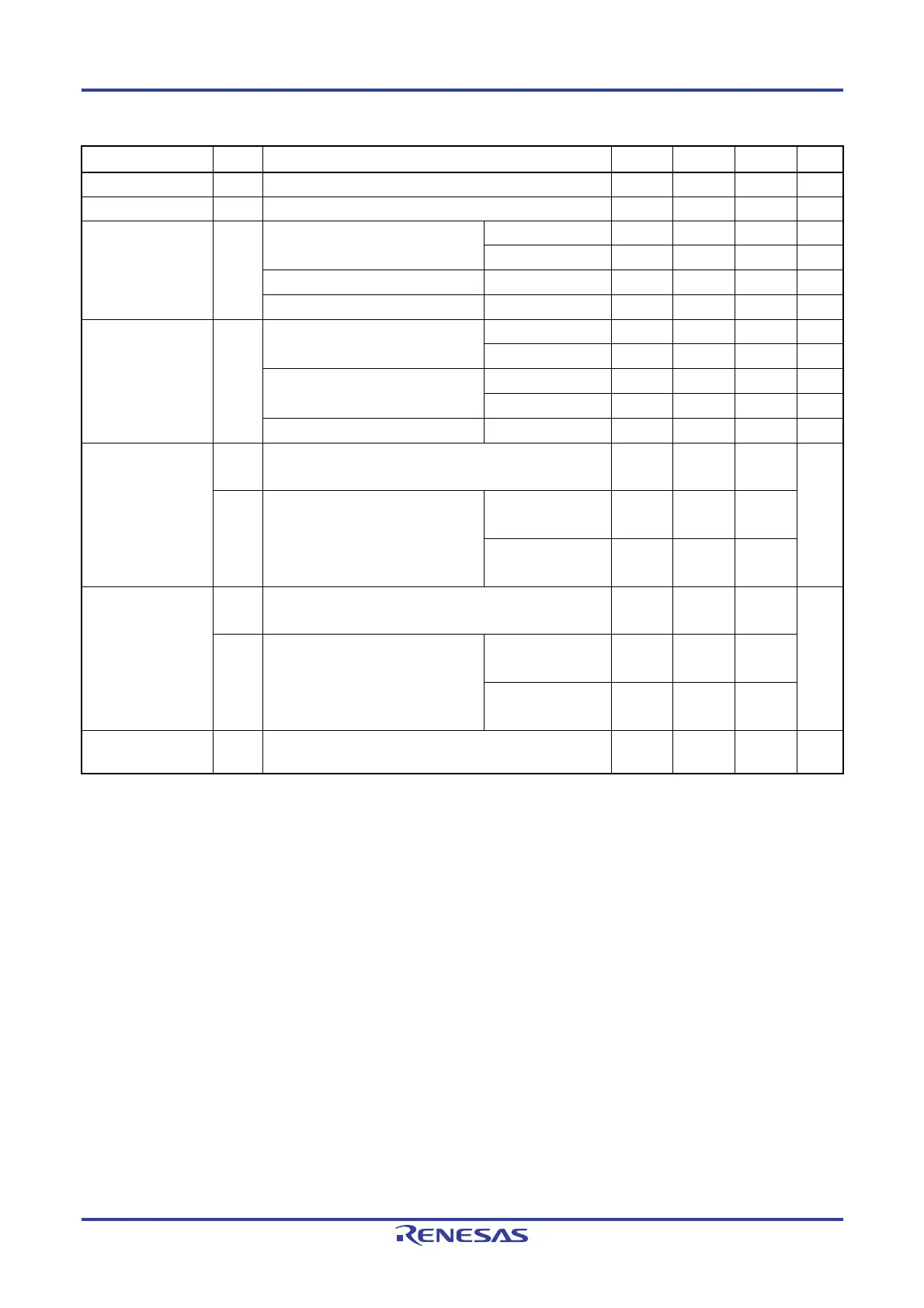
(TA = −40 to +85°C, 2.0 V ≤ VDD ≤ 5.5 V, VSS = 0 V) (2/2)
Parameter Symbol Conditions
MIN. TYP. MAX. Unit
Input voltage, high
V
IH1 0.8 VDD VDD V
Input voltage, low
V
IL1 0 0.2 VDD V
Output voltage, high
Note 1
V
OH1 4.0 V ≤ VDD ≤ 5.5 V IOH = -10 mA VDD - 1.5 V
IOH = -3.0 mA VDD - 0.7 V
2.7 V ≤ VDD ≤ 5.5 V IOH = -2.0 mA VDD - 0.6 V
2.0 V ≤ VDD ≤ 5.5 V IOH = -1.5 mA VDD - 0.5 V
Output voltage, low
Note 2
V
OL1 4.0 V ≤ VDD ≤ 5.5 V IOL = 20 mA 1.3 V
IOL = 8.5 mA 0.7 V
2.7 V ≤ VDD ≤ 5.5 V IOL = 3.0 mA 0.6 V
IOL = 1.5 mA 0.4 V
2.0 V ≤ VDD ≤ 5.5 V IOL = 0.6 mA 0.4 V
Input leakage
current, high
I
LIH1 P00 to P07, P40, P41, P125, P137
V
I = VDD
1 µA
ILIH2 P121, P122 (X1, X2, EXCLK)
V
I = VDD
In input port or
external clock input
1
In resonator
connection
10
Input leakage
current, low
I
LIL1 P00 to P07, P40, P41, P125, P137
V
I = VSS
-1 µA
ILIL2 P121, P122 (X1, X2, EXCLK)
V
I = VSS
In input port or
external clock input
-1
In resonator
connection
-10
On-chip pull-up
resistance
R
U VI = VSS 10 20 100 kΩ
Notes 1. The value under the condition which satisfies the high-level output current (I
OH1).
2. The value under the condition which satisfies the low-level output current (I
OL1).
Caution The maximum value of V
IH of P00, P01, P06, and P07 is VDD even in N-ch open-drain mode.
P00, P01, P06, and P07 do not output high level in N-ch open-drain mode.
Remark Unless specified otherwise, the characteristics of alternate-function pins are the same as those of the port.

 Loading...


