2 Operation and Features
54 Keysight U8903B User’s Guide
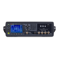
Measurement
A simplified U8903B analog analyzer block diagram is shown as follows.
Figure 2-2 U8903B analog analyzer block diagram
An audio signal can enter the analog analyzer through either the balanced (XLR) or
unbalanced (BNC) input signal connector. There is also a loopback facility where the
analog generator can be connected onto the systems internal analog bus and routed to the
analog analyzer.
From the input connector, the signal passes through the AC/DC coupling circuit. If AC
coupling is selected, the DC component is blocked and only the AC component of the
signal passes through. However, if DC coupling is selected, the entire signal
passes through.
The attenuators, buffer, gain, and common mode rejection (CMR) conditions the signal to
as close to the full scale of the analog-to-digital converter (ADC) as possible, optimizing
the measurement dynamic range.
There are two separate ADCs in the analog analyzer. The low bandwidth ADC is designed
for best performance in the audio bandwidth and beyond. The high bandwidth ADC is
designed to give high resolution measurements up to 1.5 MHz.
The default input impedance is 100 kΩ for unbalanced signals or 200 kΩ for balanced
signals. Terminations of 600 Ω or 300 Ω can also be applied. The 600 Ω termination can
tolerate up to 1.5 W and the 300 Ω termination can tolerate up to 3 W.
ANALOG ANALYZER
ADCFILTERRANGING
LOOPBACK
BNC
XLR
600 Ω 300 Ω 200 kΩ
Termination
AC/DC
Coupling
100 kΩ