RL78/G10 CHAPTER 10 A/D CONVERTER
R01UH0384EJ0311 Rev. 3.11 246
Dec 22, 2016
Table 10-1. Settings of ADCS and ADCE Bits
ADCS ADCE A/D Conversion Operation
0 0 Conversion stopped state
0 1 Conversion standby state
1 0 Setting prohibited
1 1 Conversion-in-progress state
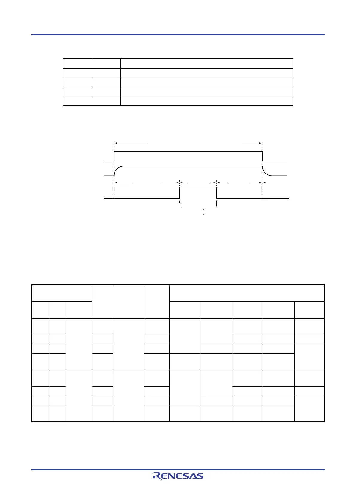
Figure 10-4. Timing Chart When A/D Voltage Comparator Is Used
ADCE
ADCS
A/D voltage comparator
Conversion
stopped
Conversion
standby
Note
1 is written
to ADCS.
0 is written to ADCS.
Conversion
standby
A/D voltage comparator: enables operation
Conversion
operation
The flag is cleared when A/D conversion ends.
Note It requires at least 0.1 μs to stabilize the internal circuit until the A/D conversion operation is started (ADCS = 1)
after the operation of the A/D voltage comparator is enabled (ADCE = 1). If the ADCS bit is set to 1 without
waiting for at least 0.1 μs, ignore data of the first conversion.
Table 10-2. 10-Bit Resolution A/D Conversion Time Selection
A/D Converter Mode
Register 0 (ADM0)
Conversion
Clock
Number of
Conversion
Clock
Conversion
Time
Conversion Time Selection (μs)
FR1 FR0 LV0
Note 2
f
CLK =
1.25 MHz
fCLK =
2.5 MHz
fCLK =
5 MHz
fCLK =
10 MHz
fCLK =
20 MHz
Note 1
0 0 0 fCLK/8 23 fAD
(Number of
sampling
clock: 9 f
AD)
184/f
CLK
Setting
prohibited
Setting
prohibited
Setting
prohibited
18.4 9.2
0 1 fCLK/4 92/fCLK 18.4 9.2 4.6
1 0 fCLK/2 46/fCLK 18.4 9.2 4.6
Setting
prohibited
1 1 fCLK 23/fCLK 18.4 9.2 4.6
Setting
prohibited
0 0 1
Note 1
fCLK/8 17 fAD
(Number of
sampling
clock: 3
f
AD)
136/f
CLK
Setting
prohibited
Setting
prohibited
Setting
prohibited
13.6 6.8
0 1 fCLK/4 68/fCLK 13.6 6.8 3.4
1 0 fCLK/2 34/fCLK 13.6 6.8 3.4
Setting
prohibited
1 1 fCLK 17/fCLK 13.6 6.8 3.4
Setting
prohibited
Notes 1. Setting prohibited when 2.4 V ≤ V
DD < 2.7 V. Can be selected when 2.7 V ≤ VDD ≤ 5.5 V.
2. When the internal reference voltage is selected as the target for conversion by the A/D converter, be sure
to clear the LV0 bit to 0.

 Loading...


