RL78/G10 CHAPTER 12 SERIAL ARRAY UNIT
R01UH0384EJ0311 Rev. 3.11 390
Dec 22, 2016
(1) Register setting
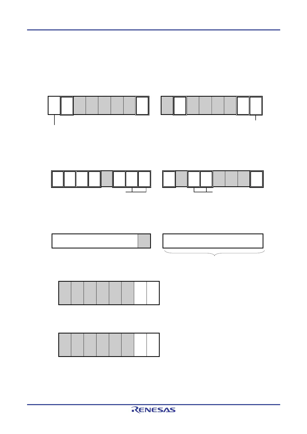
Figure 12-86. Example of Contents of Registers for Address Field Transmission of Simplified I
2
C
(IIC00) (1/2)
(a) Serial mode register 0n (SMR0nH, SMR0nL)
Symbol: SMR0nH Symbol: SMR0nL
15 14 13 12 11 10 9 8 7 6 5 4 3 2 1 0
CKS0n
0/1
CCS0n
0
0
0
0
0
0
STS0n
0
0
SIS0n0
0
1
0
0
0
MD0n1
0
MD0n0
0
Operation mode of channel n
0: Transfer end interrupt
Operation clock (fMCK) of channel n
0: Prescaler output clock CK00 set by the SPS0 register
1: Prescaler output clock CK01 set by the SPS0 register
(b) Serial communication operation setting register 0n (SCR0nH, SCR0nL)
Symbol: SCR0nH Symbol: SCR0nL
15 14 13 12 11 10 9 8 7 6 5 4 3 2 1
TXE0n
1
RXE0n
0
DAP0n
0
CKP0n
0
0
EOC0n
0
PTC0n1
0
PTC0n0
0
DIR0n
0
0
SLC0n1
0
SLC0n0
1
0
1
1
DLS0n0
1
Setting of parity bit
00B: No parity
Setting of stop bit
01B: Appending 1 bit (ACK)
(c) Serial data register 0n (SDR0nH, SDR0nL)
Symbol: SDR0nH Symbol: SDR0nL
15 14 13 12 11 10 9 8 7 6 5 4 3 2 1 0
Baud rate setting
0
Transmit data setting (address + R/W)
(d) Serial clock output register 0 (CKO0)
(e) Serial output register 0 (SO0)
(Note and Remarks are listed on the next page.)
Symbol: 7 6 5 4 3 2 1 0
CKO0
0
0
0
0
0
0
CKO01
Note
×
CKO00
0/1
Symbol: 7 6 5 4 3 2 1 0
SO0
0
0
0
0
0
0
SO01
Note
×
SO00
0/1
Start condition is generated by manipulating the SO0n bit.
SIOr

 Loading...


