RM0401 Rev 3 143/771
RM0401 General-purpose I/Os (GPIO)
154
6.3.10 Output configuration
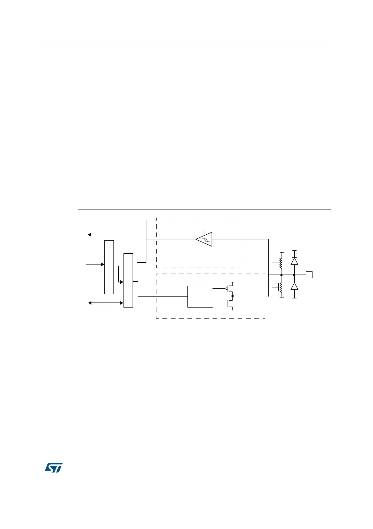
When the I/O port is programmed as output:
• The output buffer is enabled:
– Open drain mode: A “0” in the Output register activates the N-MOS whereas a “1”
in the Output register leaves the port in Hi-Z (the P-MOS is never activated)
– Push-pull mode: A “0” in the Output register activates the N-MOS whereas a “1” in
the Output register activates the P-MOS
• The Schmitt trigger input is activated
• The weak pull-up and pull-down resistors are activated or not depending on the value
in the GPIOx_PUPDR register
• The data present on the I/O pin are sampled into the input data register every AHB1
clock cycle
• A read access to the input data register gets the I/O state
• A read access to the output data register gets the last written value
Figure 19 shows the output configuration of the I/O port bit.
Figure 19. Output configuration
6.3.11 Alternate function configuration
When the I/O port is programmed as alternate function:
• The output buffer can be configured as open-drain or push-pull
• The output buffer is driven by the signal coming from the peripheral (transmitter enable
and data)
• The Schmitt trigger input is activated
• The weak pull-up and pull-down resistors are activated or not depending on the value
in the GPIOx_PUPDR register
• The data present on the I/O pin are sampled into the input data register every AHB1
clock cycle
• A read access to the input data register gets the I/O state
Figure 20 shows the Alternate function configuration of the I/O port bit.
0USHPULLOR
/PENDRAIN
/UTPUT
CONTROL
6
$$
6
33
44,3CHMITT
TRIGGER
ON
)NPUTDRIVER
/UTPUTDRIVER
0-/3
.-/3
)NPUTDATAREGISTER
/UTPUTDATAREGISTER
2EADWRITE
2EAD
"ITSETRESETREGISTERS
7RITE
ONOFF
PULL
PULL
ONOFF
6
$$
6
33
6
33
6
$$
PROTECTION
DIODE
PROTECTION
DIODE
DOWN
UP
)/PIN
AIB