RM0401 Rev 3 745/771
RM0401 Debug support (DBG)
762
26.8.6 SW-AP registers
Access to these registers are initiated when APnDP=1
There are many AP Registers (see AHB-AP) addressed as the combination of:
• The shifted value A[3:2]
• The current value of the DP SELECT register
26.9 AHB-AP (AHB access port) - valid for both JTAG-DP
and SW-DP
Features:
• System access is independent of the processor status.
• Either SW-DP or JTAG-DP accesses AHB-AP.
• The AHB-AP is an AHB master into the Bus Matrix. Consequently, it can access all the
data buses (Dcode Bus, System Bus, internal and external PPB bus) but the ICode
bus.
• Bitband transactions are supported.
• AHB-AP transactions bypass the FPB.
The address of the 32-bits AHP-AP resisters are 6-bits wide (up to 64 words or 256 bytes)
and consists of:
d) Bits [7:4] = the bits [7:4] APBANKSEL of the DP SELECT register
e) Bits [3:2] = the 2 address bits of A[3:2] of the 35-bit packet request for SW-DP.
The AHB-AP of the Cortex
®
-M4 with FPU includes 9 x 32-bits registers:
Refer to the Cortex
®
-M4 with FPU r0p1 TRM for further details.
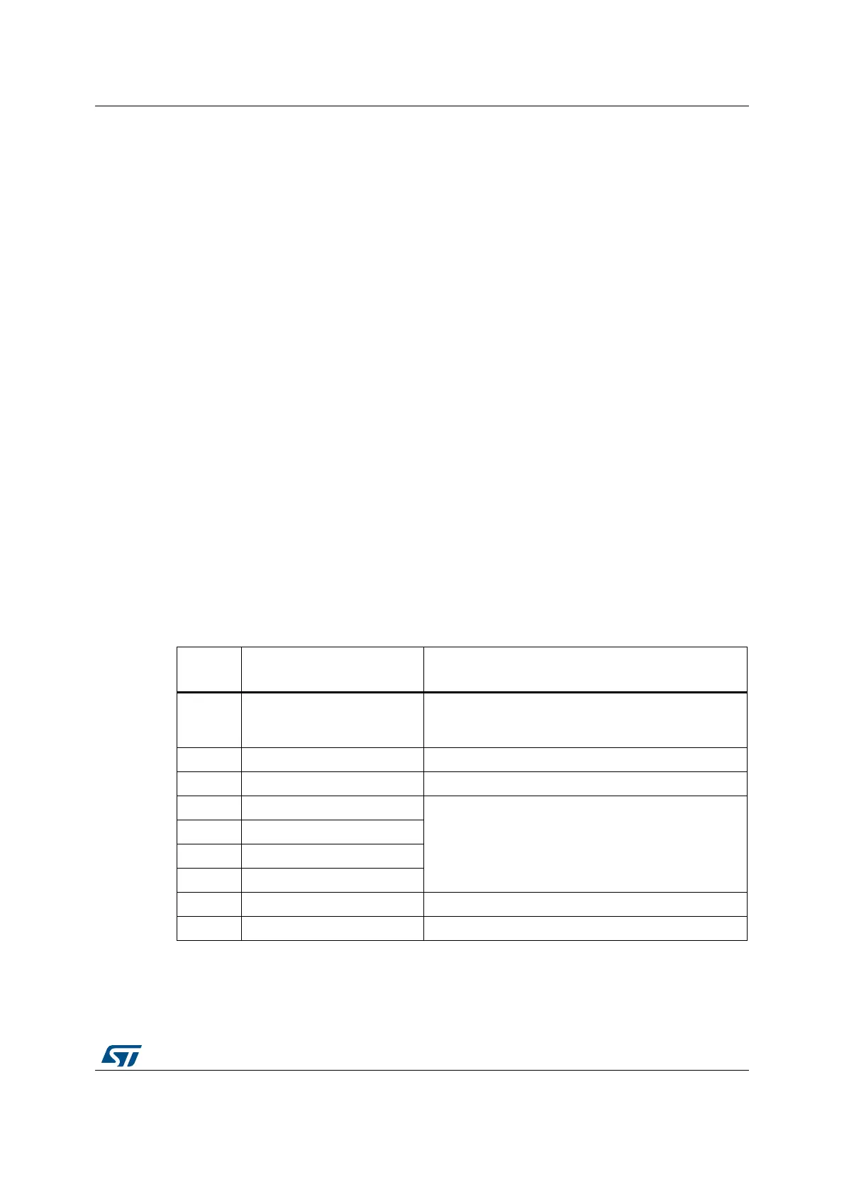
Table 137. Cortex
®
-M4 with FPU AHB-AP registers
Address
offset
Register name Notes
0x00
AHB-AP Control and Status
Word
Configures and controls transfers through the AHB
interface (size, hprot, status on current transfer, address
increment type
0x04 AHB-AP Transfer Address -
0x0C AHB-AP Data Read/Write -
0x10 AHB-AP Banked Data 0
Directly maps the 4 aligned data words without rewriting
the Transfer Address Register.
0x14 AHB-AP Banked Data 1
0x18 AHB-AP Banked Data 2
0x1C AHB-AP Banked Data 3
0xF8 AHB-AP Debug ROM Address Base Address of the debug interface
0xFC AHB-AP ID Register -