Analog-to-digital converter (ADC) RM0401
240/771 RM0401 Rev 3
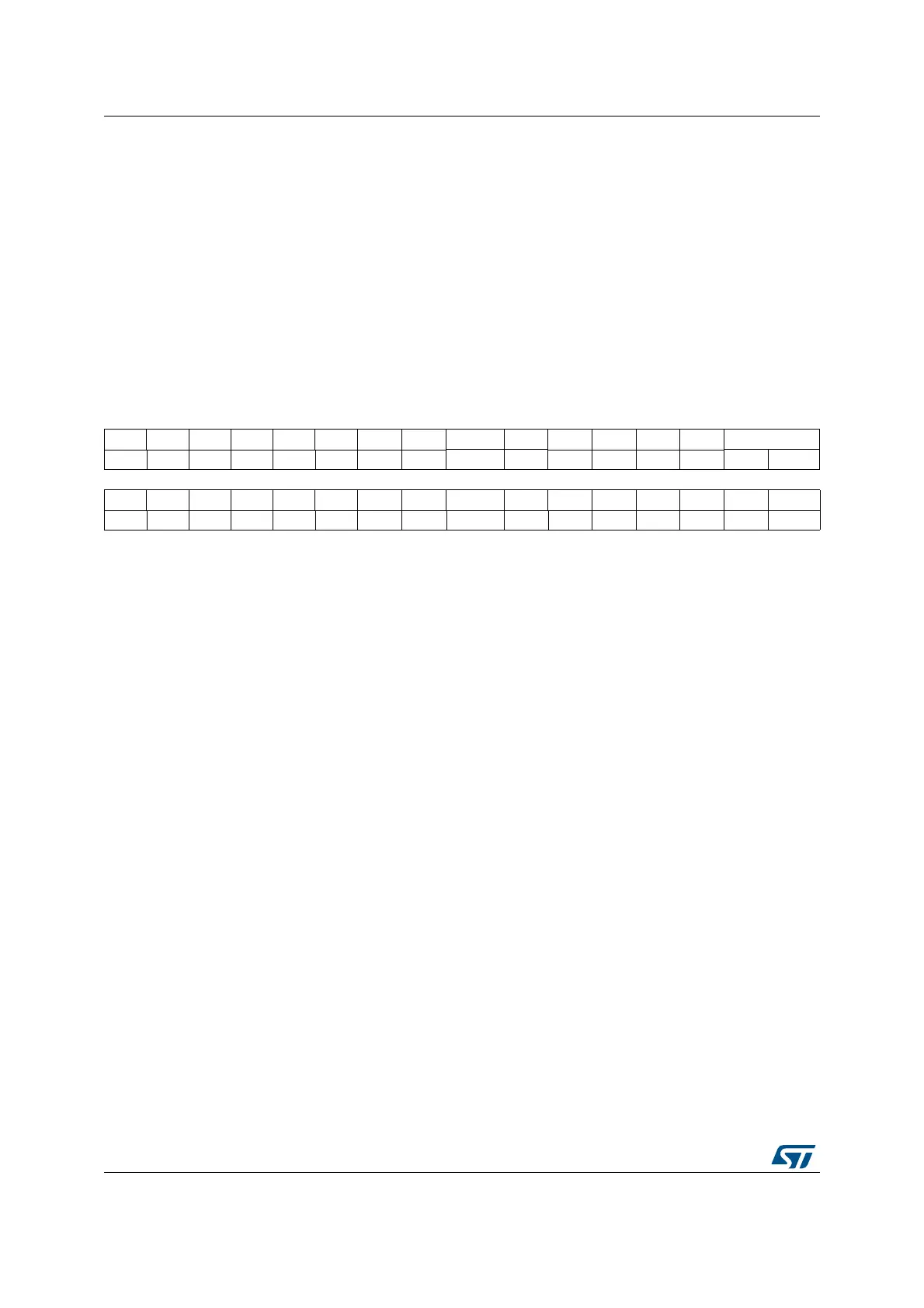
11.12.16 ADC common control register (ADC_CCR)
Address offset: 0x04 (this offset address is relative to ADC1 base address + 0x300)
Reset value: 0x0000 0000
Bit 2 JEOC1: Injected channel end of conversion of ADC1
This bit is a copy of the JEOC bit in the ADC1_SR register.
Bit 1 EOC1: End of conversion of ADC1
This bit is a copy of the EOC bit in the ADC1_SR register.
Bit 0 AWD1: Analog watchdog flag of ADC1
This bit is a copy of the AWD bit in the ADC1_SR register.
31 30 29 28 27 26 25 24 23 22 21 20 19 18 17 16
Res. Res. Res. Res. Res. Res. Res. Res. TSVREFE VBATE Res. Res. Res. Res. ADCPRE
rw rw rw rw
15 14 13 12 11 10 9 8 7 6 5 4 3 2 1 0
Res. Res. Res. Res. Res. Res. Res. Res. Res. Res. Res. Res. Res. Res. Res. Res.
Bits 31:24 Reserved, must be kept at reset value.
Bit 23 TSVREFE: Temperature sensor and V
REFINT
enable
This bit is set and cleared by software to enable/disable the temperature sensor and the
V
REFINT
channel.
0: Temperature sensor and V
REFINT
channel disabled
1: Temperature sensor and V
REFINT
channel enabled
Note: VBATE must be disabled when TSVREFE is set. If both bits are set, only the VBAT
conversion is performed.
Bit 22 VBATE: V
BAT
enable
This bit is set and cleared by software to enable/disable the V
BAT
channel.
0: V
BAT
channel disabled
1: V
BAT
channel enabled
Bits 21:18 Reserved, must be kept at reset value.
Bits 17:16 ADCPRE: ADC prescaler
Set and cleared by software to select the frequency of the clock to the ADC. The clock is
common for all the ADCs.
Note: 00: PCLK2 divided by 2
01: PCLK2 divided by 4
10: PCLK2 divided by 6
11: PCLK2 divided by 8
Bits 15:0 Reserved, must be kept at reset value.