System configuration controller (SYSCFG) RM0401
156/771 RM0401 Rev 3
7.2.2 SYSCFG peripheral mode configuration register (SYSCFG_PMC)
Address offset: 0x04
Reset value: 0x0000 0000
Bits 31:2 Reserved, must be kept at reset value.
Bits 1:0 MEM_MODE: Memory mapping selection
Set and cleared by software. This bit controls the memory internal mapping at
address 0x0000 0000. After reset these bits take the value selected by the Boot
pins.
00: Main Flash memory mapped at 0x0000 0000
01: System Flash memory mapped at 0x0000 0000
10: reserved
11: Embedded SRAM mapped at 0x0000 0000
Note: Refer to
Figure 2: Memory map for details about the memory mapping at
address 0x0000 0000.
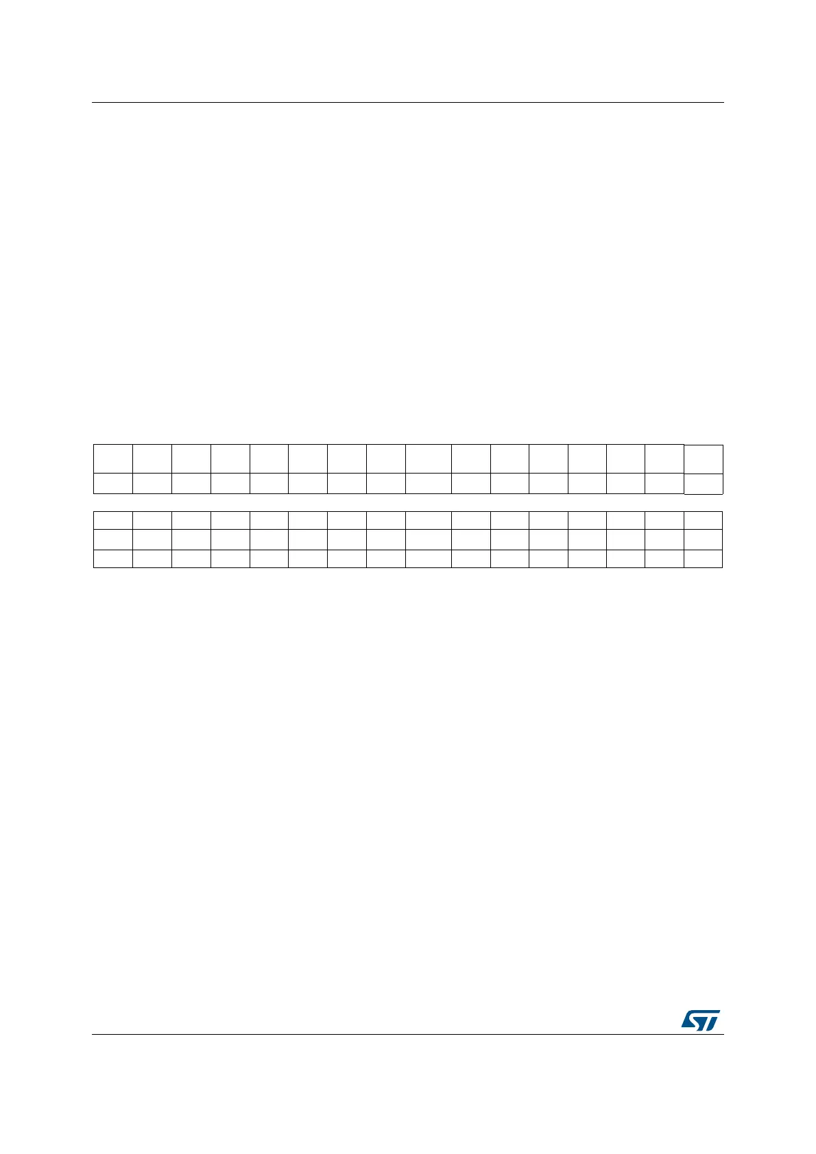
31 30 29 28 27 26 25 24 23 22 21 20 19 18 17 16
Res. Res. Res. Res. Res. Res. Res. Res. Res. Res. Res. Res. Res. Res. Res.
ADC1D
C2
rw
15 14 13 12 11 10 9 8 7 6 5 4 3 2 1 0
Res. Res. Res. Res. Res. Res. Res. Res. Res. Res. Res. Res. Res. Res. Res. Res.
Res. Res. Res. Res. Res. Res. Res. Res. Res. Res. Res. Res. Res. Res. Res. Res.
Bits 31:17 Reserved, must be kept at reset value.
Bit 16 ADC1DC2:
0: No effect.
1: Refer to AN4073 on how to use this bit
Note: These bits can be set only if the following conditions are met:
- ADC clock higher or equal to 30 MHz.
- Only one ADC1DC2 bit must be selected if ADC conversions do not start
at the same time and the sampling times differ.
- These bits must not be set when the ADCDC1 bit is set in PWR_CR
register.
Bits 15:0 Reserved, must be kept at reset value.