RM0401 Rev 3 675/771
RM0401 Universal synchronous receiver transmitter (USART) /universal asynchronous receiver
679
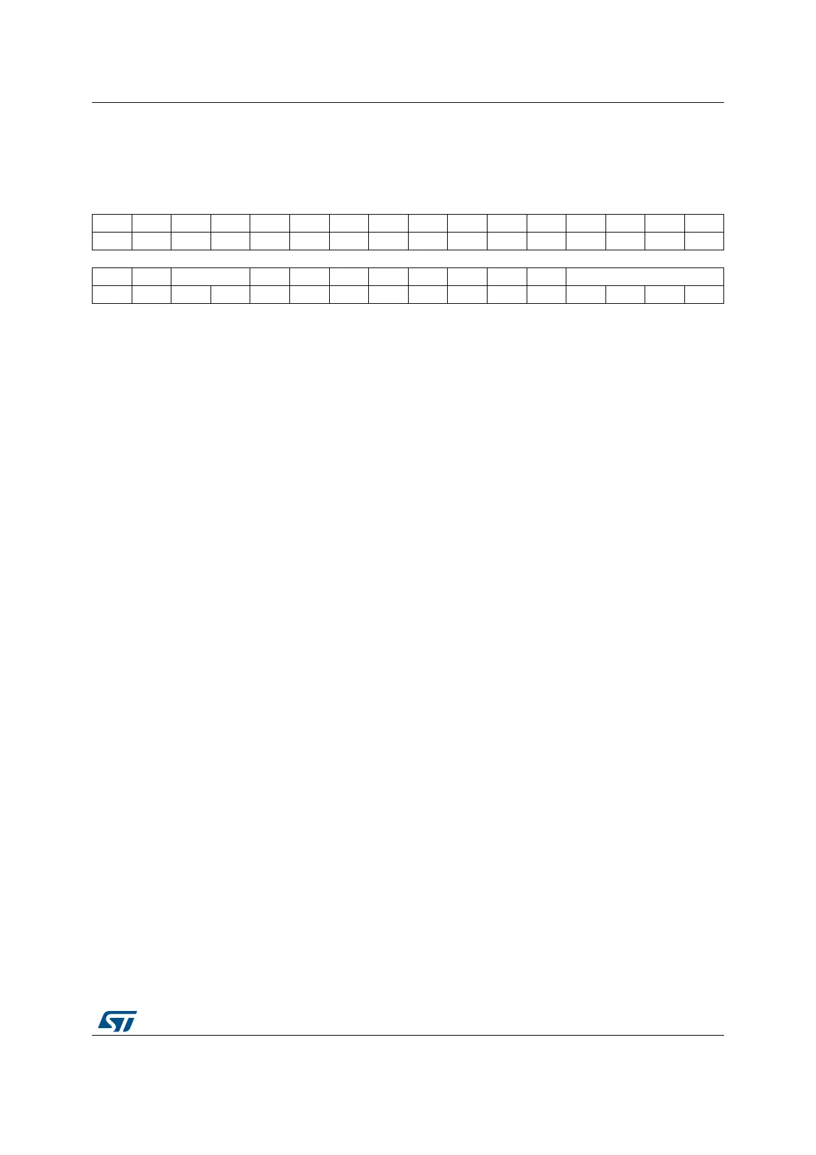
24.6.5 Control register 2 (USART_CR2)
Address offset: 0x10
Reset value: 0x0000 0000
31 30 29 28 27 26 25 24 23 22 21 20 19 18 17 16
Res. Res. Res. Res. Res. Res. Res. Res. Res. Res. Res. Res. Res. Res. Res. Res.
1514131211109876543210
Res. LINEN STOP[1:0] CLKEN CPOL CPHA LBCL Res. LBDIE LBDL Res. ADD[3:0]
rw rw rw rw rw rw rw rw rw rw rw rw rw
Bits 31:15 Reserved, must be kept at reset value
Bit 14 LINEN: LIN mode enable
This bit is set and cleared by software.
0: LIN mode disabled
1: LIN mode enabled
The LIN mode enables the capability to send LIN Synch Breaks (13 low bits) using the SBK bit in
the USART_CR1 register, and to detect LIN Sync breaks.
Bits 13:12 STOP: STOP bits
These bits are used for programming the stop bits.
00: 1 Stop bit
01: 0.5 Stop bit
10: 2 Stop bits
11: 1.5 Stop bit
Note: The 0.5 Stop bit and 1.5 Stop bit are not available for UART4 & UART5.
Bit 11 CLKEN: Clock enable
This bit allows the user to enable the SCLK pin.
0: SCLK pin disabled
1: SCLK pin enabled
This bit is not available for UART4 & UART5.
Bit 10 CPOL: Clock polarity
This bit allows the user to select the polarity of the clock output on the SCLK pin in synchronous
mode. It works in conjunction with the CPHA bit to produce the desired clock/data relationship
0: Steady low value on SCLK pin outside transmission window.
1: Steady high value on SCLK pin outside transmission window.
This bit is not available for UART4 & UART5.
Bit 9 CPHA: Clock phase
This bit allows the user to select the phase of the clock output on the SCLK pin in synchronous
mode. It works in conjunction with the CPOL bit to produce the desired clock/data relationship (see
figures 226 to 227)
0: The first clock transition is the first data capture edge
1: The second clock transition is the first data capture edge
Note: This bit is not available for UART4 & UART5.