RM0401 Rev 3 691/771
RM0401 Serial peripheral interface/ inter-IC sound (SPI/I2S)
731
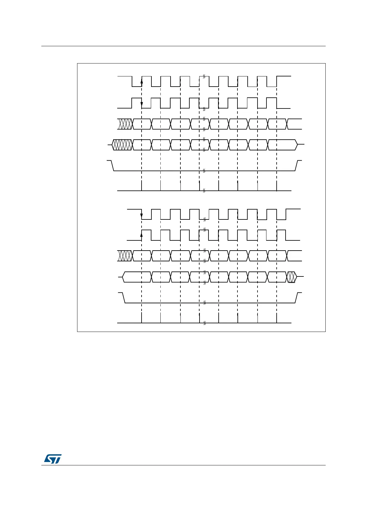
Figure 246. Data clock timing diagram
Note: The order of data bits depends on LSBFIRST bit setting.
Data frame format
The SPI shift register can be set up to shift out MSB-first or LSB-first, depending on the
value of the LSBFIRST bit. Each data frame is 8 or 16 bit long depending on the size of the
data programmed using the DFF bit in the SPI_CR1 register. The selected data frame
format is applicable both for transmission and reception.
&32/
&32/
06%LW
/6%LW
06%LW
/6%LW
0,62
026,
166
WRVODYH
&DSWXUHVWUREH
&3+$
&32/
&32/
06%LW
/6%LW
06%LW
/6%LW
0,62
026,
166
WRVODYH
&DSWXUHVWUREH
&3+$
DLG