Debug support (DBG) RM0401
734/771 RM0401 Rev 3
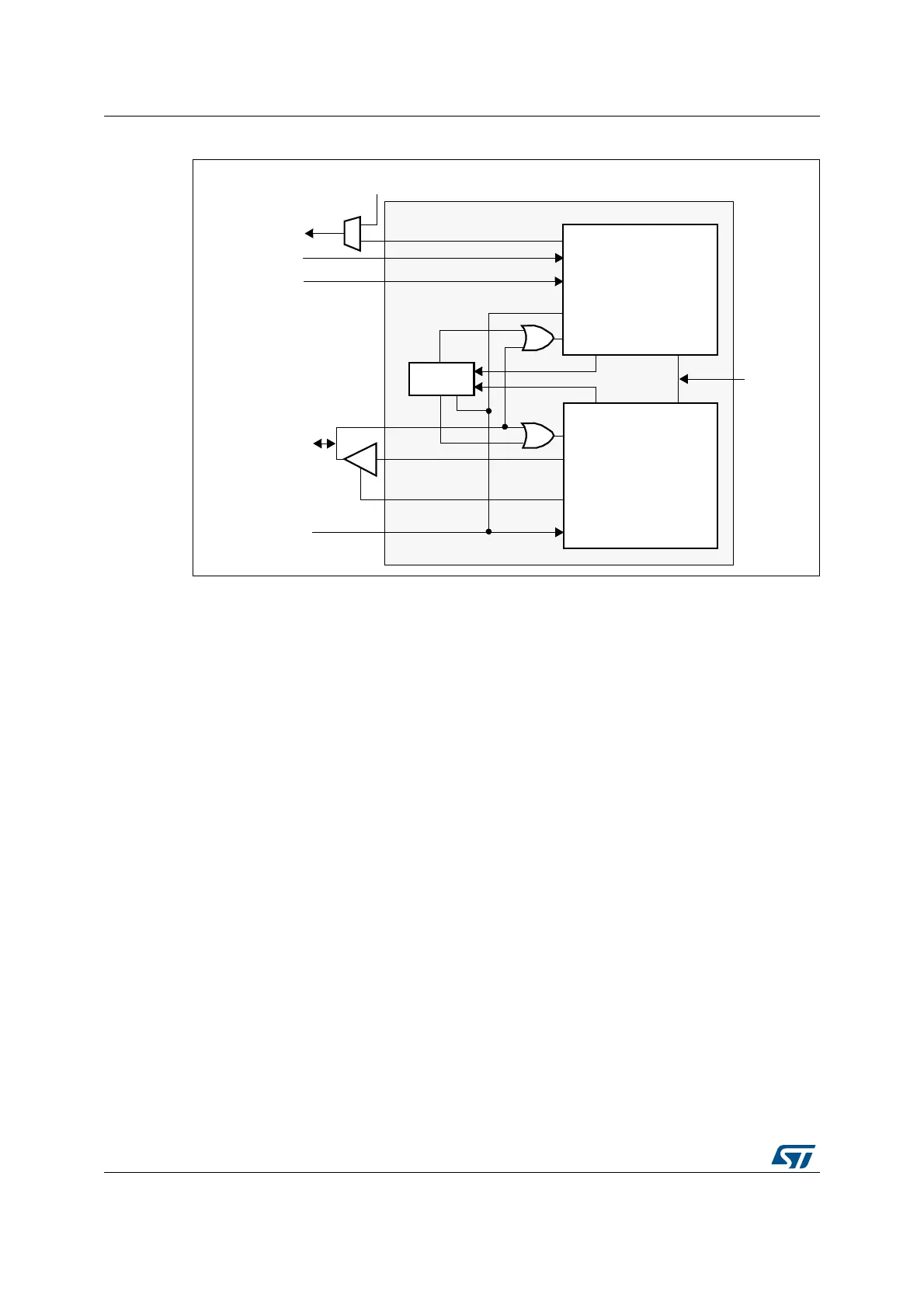
Figure 274. SWJ debug port
Figure 274 shows that the asynchronous TRACE output (TRACESWO) is multiplexed with
TDO. This means that the asynchronous trace can only be used with SW-DP, not JTAG-DP.
26.3.1 Mechanism to select the JTAG-DP or the SW-DP
By default, the JTAG-Debug Port is active.
If the debugger host wants to switch to the SW-DP, it must provide a dedicated JTAG
sequence on TMS/TCK (respectively mapped to SWDIO and SWCLK) which disables the
JTAG-DP and enables the SW-DP. This way it is possible to activate the SWDP using only
the SWCLK and SWDIO pins.
This sequence is:
1. Send more than 50 TCK cycles with TMS (SWDIO) =1
2. Send the 16-bit sequence on TMS (SWDIO) = 0111100111100111 (MSB transmitted
first)
3. Send more than 50 TCK cycles with TMS (SWDIO) =1
26.4 Pinout and debug port pins
The STM32F410 MCUs are available in various packages with different numbers of
available pins. As a result, some functionality (ETM) related to pin availability may differ
between packages.
TRACESWO
JTDO
JTDI
NJTRST
nTRST
TDI
TDO
SWJ-DP
TDO
TDI
nTRST
TCK
TMS
nPOTRST
JTAG-DP
nPOTRST
From
power-on
reset
DBGRESETn
DBGDI
DBGDO
DBGDOEN
DBGCLK
SW-DP
SWCLKTCK
SWDOEN
SWDO
SWDITMS
SWD/JTAG
select
JTMS/SWDIO
JTCK/SWCLK
(asynchronous trace)
ai17139