Digital-to-analog converter (DAC) RM0401
246/771 RM0401 Rev 3
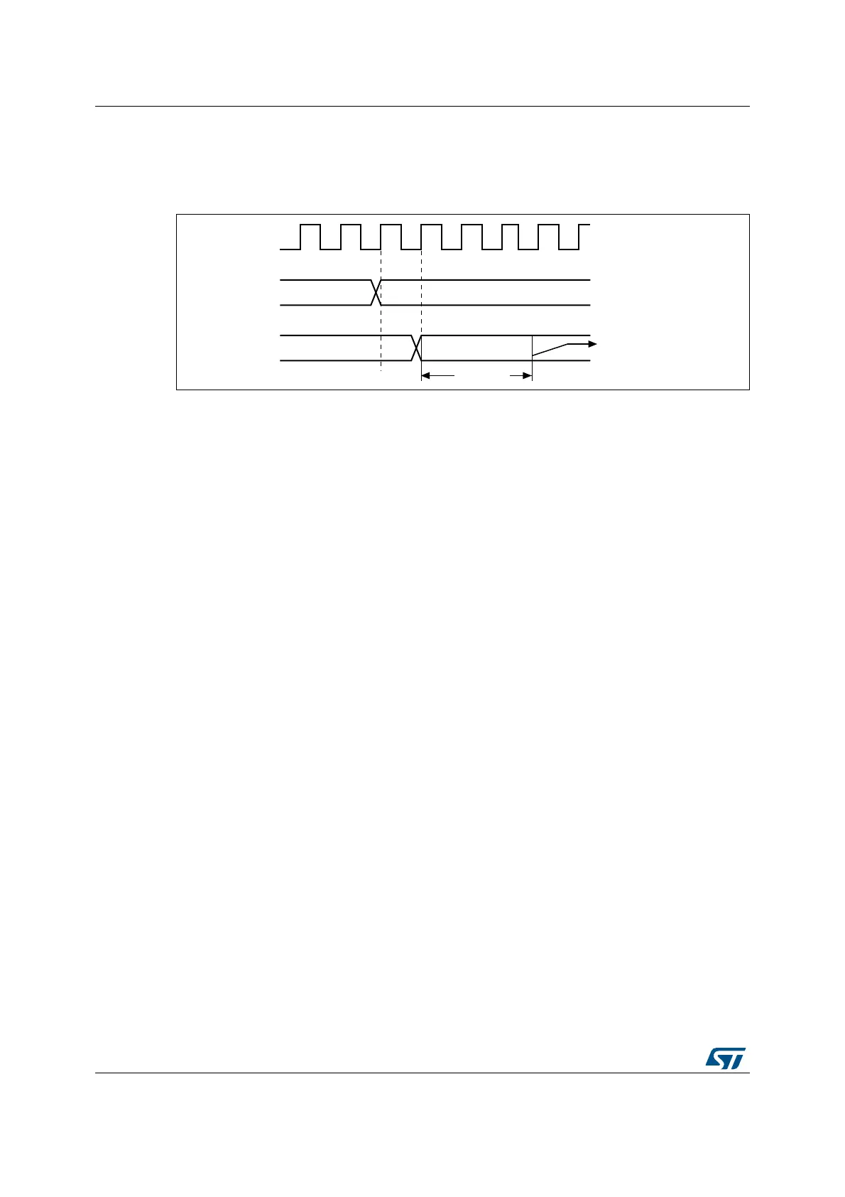
When DAC_DORx is loaded with the DAC_DHRx contents, the analog output voltage
becomes available after a time t
SETTLING
that depends on the power supply voltage and the
analog output load.
Figure 42. Timing diagram for conversion with trigger disabled TEN = 0
Independent trigger with single LFSR generation
To configure the DAC in this conversion mode (see Section 12.6: Noise generation), the
following sequence is required:
1. Set the DAC channel trigger enable bit TENx.
2. Configure the trigger source by setting TSELx[2:0] bits.
3. Configure the DAC channel WAVEx[1:0] bits as “01” and the same LFSR mask value in
the MAMPx[3:0] bits
4. Load the DAC channel data into the desired DAC_DHRx register (DHR12RD,
DHR12LD or DHR8RD).
When a DAC channelx trigger arrives, the LFSRx counter, with the same mask, is added to
the DHRx register and the sum is transferred into DAC_DORx (three APB clock cycles
later). Then the LFSRx counter is updated.
Independent trigger with single triangle generation
To configure the DAC in this conversion mode (see Section 12.7: Triangle-wave generation),
the following sequence is required:
1. Set the DAC channelx trigger enable TENx bits.
2. Configure the trigger source by setting TSELx[2:0] bits.
3. Configure the DAC channelx WAVEx[1:0] bits as “1x” and the same maximum
amplitude value in the MAMPx[3:0] bits
4. Load the DAC channelx data into the desired DAC_DHRx register. (DHR12RD,
DHR12LD or DHR8RD).
When a DAC channelx trigger arrives, the DAC channelx triangle counter, with the same
triangle amplitude, is added to the DHRx register and the sum is transferred into
DAC_DORx (three APB clock cycles later). The DAC channelx triangle counter is then
updated.
!0"?#,+
X!#
X!#
T
3%44,).'
$(2
$/2
/UTPUTVOLTAGE
AVAILABLEON$!#?/54PIN
AIB