Direct memory access controller (DMA) RM0401
192/771 RM0401 Rev 3
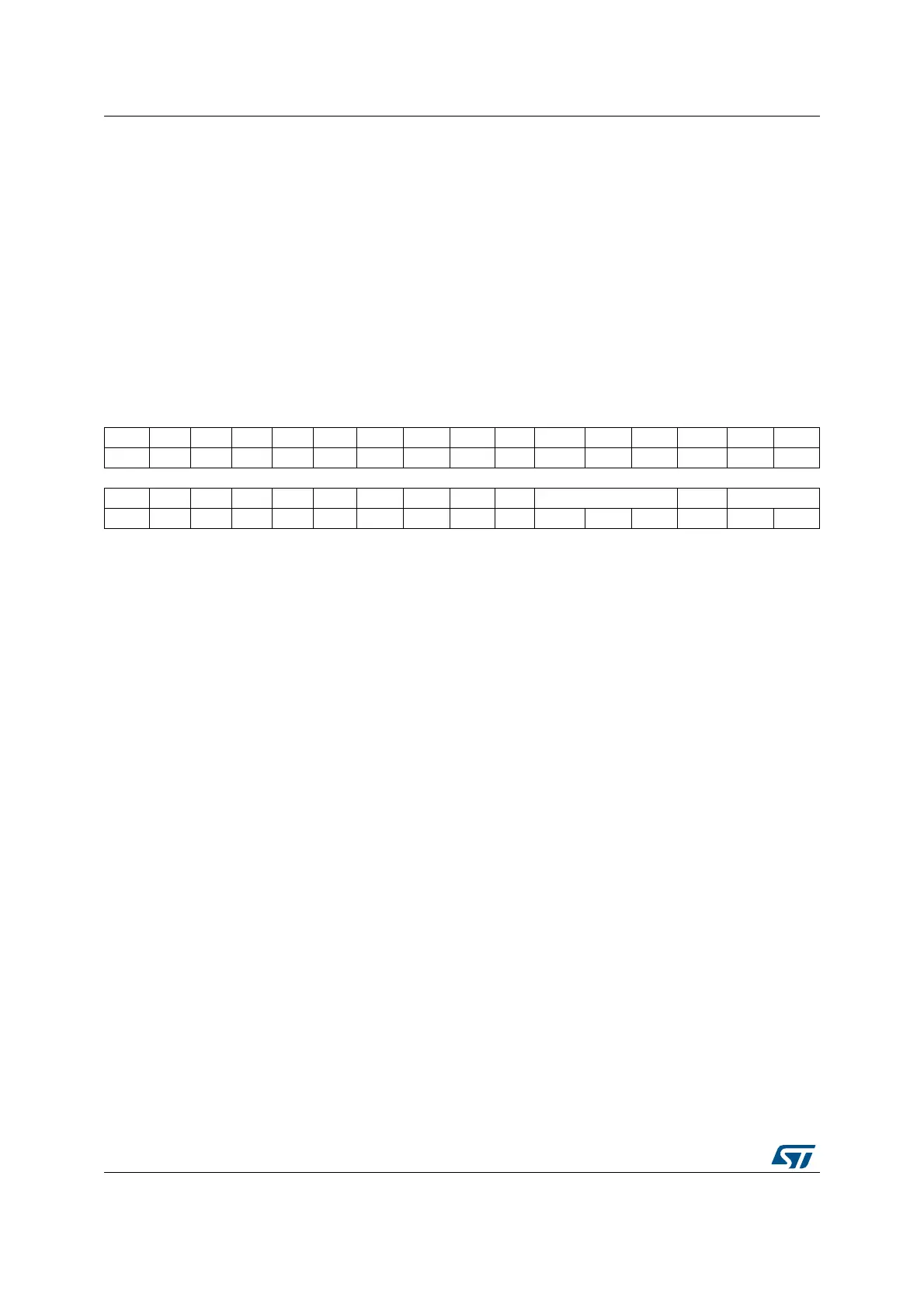
8.5.10 DMA stream x FIFO control register (DMA_SxFCR)
Address offset: 0x24 + 0x18 * x, (x = 0 to 7)
Reset value: 0x0000 0021
Bits 31:0 M1A[31:0]: memory 1 address (used in case of double-buffer mode)
Base address of memory area 1 from/to which the data is read/written.
This register is used only for the double-buffer mode.
These bits are write-protected. They can be written only if:
– the stream is disabled (bit EN= '0' in the DMA_SxCR register) or
– the stream is enabled (EN=’1’ in DMA_SxCR register) and bit CT = '0' in the
DMA_SxCR register.
31 30 29 28 27 26 25 24 23 22 21 20 19 18 17 16
Res. Res. Res. Res. Res. Res. Res. Res. Res. Res. Res. Res. Res. Res. Res. Res.
15 14 13 12 11 10 9 8 7 6 5 4 3 2 1 0
Res. Res. Res. Res. Res. Res. Res. Res. FEIE Res. FS[2:0] DMDIS FTH[1:0]
rw r r r rw rw rw
Bits 31:8 Reserved, must be kept at reset value.
Bit 7 FEIE: FIFO error interrupt enable
This bit is set and cleared by software.
0: FE interrupt disabled
1: FE interrupt enabled
Bit 6 Reserved, must be kept at reset value.
Bits 5:3 FS[2:0]: FIFO status
These bits are read-only.
000: 0 < fifo_level < 1/4
001: 1/4 ≤ fifo_level < 1/2
010: 1/2 ≤ fifo_level < 3/4
011: 3/4 ≤ fifo_level < full
100: FIFO is empty
101: FIFO is full
others: no meaning
These bits are not relevant in the direct mode (DMDIS bit is zero).
Bit 2 DMDIS: direct mode disable
This bit is set and cleared by software. It can be set by hardware.
0: direct mode enabled
1: direct mode disabled
This bit is protected and can be written only if EN is ‘0’.
This bit is set by hardware if the memory-to-memory mode is selected (DIR bit in
DMA_SxCR are “10”) and the EN bit in the DMA_SxCR register is ‘1’ because the direct
mode is not allowed in the memory-to-memory configuration.