Power controller (PWR) RM0401
86/771 RM0401 Rev 3
4.4 Power control registers
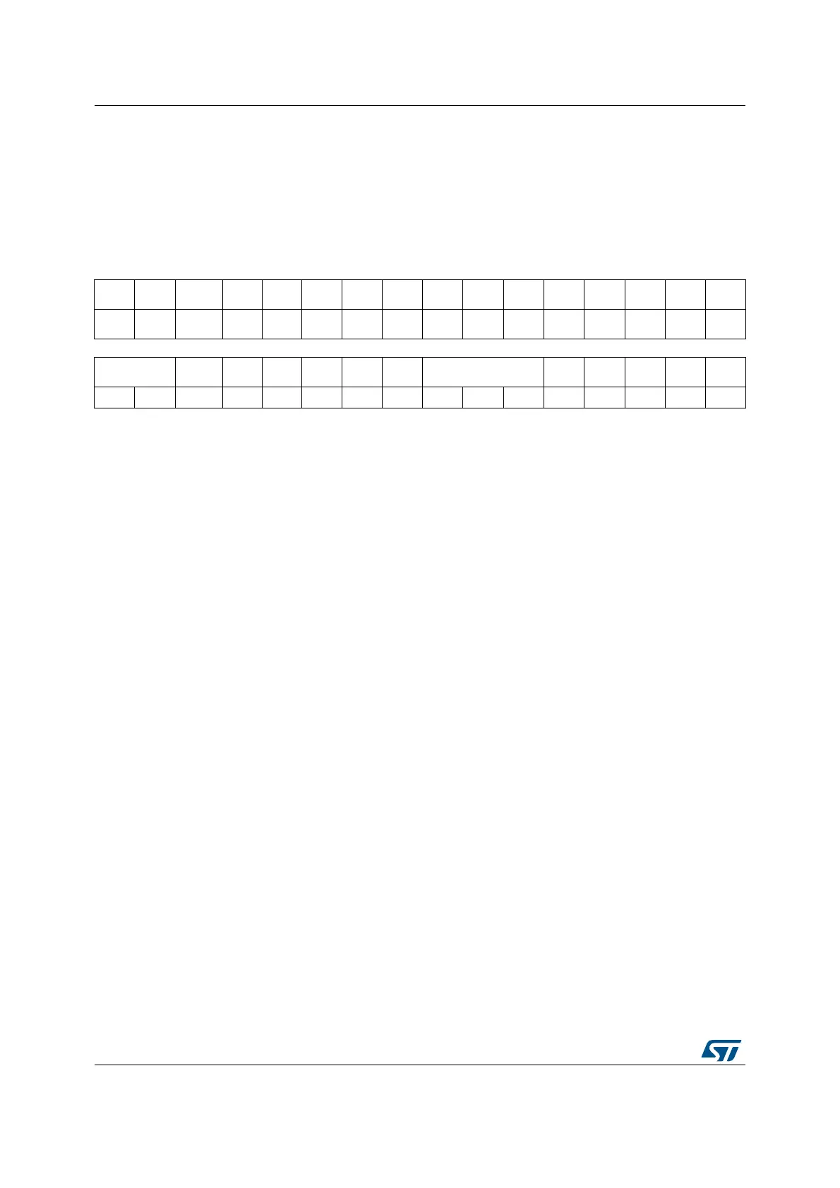
4.4.1 PWR power control register (PWR_CR)
Address offset: 0x00
Reset value: 0x0000 8000 (reset by wakeup from Standby mode)
31 30 29 28 27 26 25 24 23 22 21 20 19 18 17 16
Res. Res. Res. Res. Res. Res. Res. Res. Res. Res. FISSR FMSSR Res. Res. Res. Res.
rw rw
1514131211109876543210
VOS ADCDC1 Res.
MRLV
DS
LPLV
DS
FPDS DBP PLS[2:0] PVDE CSBF CWUF PDDS LPDS
rw rw rw rw rw rw rw rw rw rw rw w w rw rw
Bits 31:22 Reserved, must be kept at reset value.
Bit 21 FISSR: Flash Interface Stop while System Run
0: Flash Interface clock run (Default value).
1: Flash Interface clock off.
Note: This bit could not be set while executing with the Flash itself. It should be done with
specific routine executed from RAM.
Bit 20 FMSSR: Flash Memory Sleep System Run.
0: Flash standard mode (Default value)
1: Flash forced to be in STOP or Deep-power down mode (depending of FPDS value bit) by
hardware.
Note: This bit could not be set while executing with the Flash itself. It should be done with
specific routine executed from RAM.
Bits 19:16 Reserved, must be kept at reset value.
Bits 15:14 VOS[1:0]: Regulator voltage scaling output selection
These bits control the main internal voltage regulator output voltage to achieve a trade-off
between performance and power consumption when the device does not operate at the
maximum frequency (refer to the corresponding datasheet for more details).
These bits can be modified only when the PLL is OFF. The new value programmed is active
only when the PLL is ON. When the PLL is OFF, the voltage regulator is set to scale 3
independently of the VOS register content.
00: Reserved (Scale 3 mode selected)
01: Scale 3 mode <= 64 MHz
10: Scale 2 mode (reset value) <= 84 MHz
11: Scale 1 mode <= 100 MHz
Bit 13 ADCDC1:
0: No effect.
1: Refer to AN4073 for details on how to use this bit.
Note: This bit can only be set when operating at supply voltage range 2.7 to 3.6V and when
the Prefetch is OFF.