RM0401 Rev 3 159/771
RM0401 System configuration controller (SYSCFG)
161
7.2.7 SYSCFG configuration register 2 (SYSCFG_CFGR2)
Address offset: 0x1C
Reset value: 0x0000 0000
7.2.8 Compensation cell control register (SYSCFG_CMPCR)
Address offset: 0x20
Reset value: 0x0000 0000
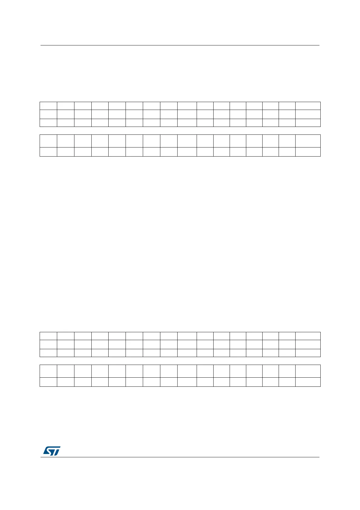
31 30 29 28 27 26 25 24 23 22 21 20 19 18 17 16
Res. Res. Res. Res. Res. Res. Res. Res. Res. Res. Res. Res. Res. Res. Res. Res.
Res. Res. Res. Res. Res. Res. Res. Res. Res. Res. Res. Res. Res. Res. Res. Res.
1514131211109 8 7 654321 0
Res. Res. Res. Res. Res. Res. Res. Res. Res. Res. Res. Res. Res. PVDL Res. CLL
rw rw
Bits 31:3 Reserved, must be kept at reset value.
Bit 8 PVDL: PVD lock
This bit is set by software. It can be cleared only by a system reset. It enables and
locks the PVD connection to TIM1 Break input. It also locks (write protection) the
PVDE and PVDS[2:0] bits of PWR_CR register.
0: PVD interrupt not connected to TIM1 Break input. PVDE and PVDS[2:0] can be
read and modified
1: PVD interrupt connected to TIM1 Break input. PVDE and PVDS[2:0] are read-only
Bit 1 Reserved, must be kept at reset value.
Bit 0 CLL: core lockup lock
This bit is set and cleared by software. It enables and locks the LOCKUP (Hardfault)
output of the Cortex-M4 core with TIM1 Break input.
0: Cortex-M4 LOCKUP output not connected to TIM1 Break input
1: Cortex-M4 LOCKUP output connected to TIM1 Break input
31 30 29 28 27 26 25 24 23 22 21 20 19 18 17 16
Res. Res. Res. Res. Res. Res. Res. Res. Res. Res. Res. Res. Res. Res. Res. Res.
Res. Res. Res. Res. Res. Res. Res. Res. Res. Res. Res. Res. Res. Res. Res. Res.
1514131211109 8 7 654321 0
Res. Res. Res. Res. Res. Res. Res. READY Res. Res. Res. Res. Res. Res. Res. CMP_PD
r rw