Digital-to-analog converter (DAC) RM0401
244/771 RM0401 Rev 3
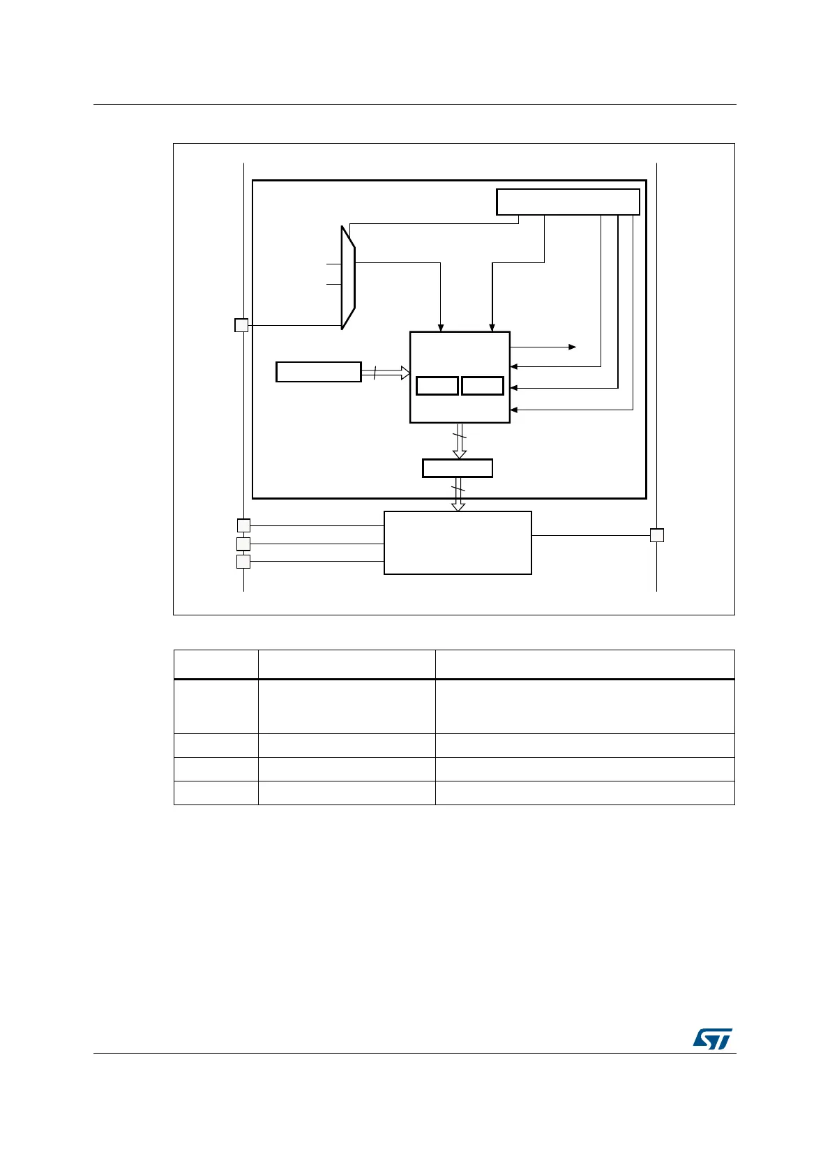
Figure 40. DAC channel block diagram
Note: Once DAC_Channelx is enabled, the corresponding GPIO pin (PA5) is automatically
connected to the analog converter output (DAC1_OUT). In order to avoid parasitic
consumption, the PA5 pin should first be configured to analog (AIN).
12.3 DAC output buffer enable
The DAC integrates one output buffer that can be used to reduce the output impedance on
DAC1_OUT1 output, and to drive external loads directly without having to add an external
operational amplifier.
Table 51. DAC pins
Name Signal type Remarks
V
REF+
Input, analog positive
reference
The higher/positive reference voltage for the DAC.
V
DDA
and V
REF+
are connected together on the
package.
V
DDA
Input, analog supply Analog power supply
V
SSA
Input, analog supply ground Ground for analog power supply
DAC1_OUT Analog output signal DAC1 channel analog output
06Y9
9
5()
'$&B287
&RQWUROORJLF[
WULDQJOH[
'0$UHTXHVW[
76(/[>@ELWV
7,0B75*2
(;7,B
'0$(1[
7(1[
:$9(1[>@ELWV
6:75,*[
ELW
'$&FRQWUROUHJLVWHU
'+5[
/)65[
'25[
'LJLWDOWRDQDORJ
FRQYHUWHU[
7ULJJHUVHOHFWRU[
9
66$
9
''$
ELW
0$03[>@ELWV