RM0401 Rev 3 43/771
RM0401
44
2.6 Boot configuration
Due to its fixed memory map, the code area starts from address 0x0000 0000 (accessed
through the ICode/DCode buses) while the data area (SRAM) starts from address
0x2000 0000 (accessed through the system bus). The Cortex
®
-M4 with FPU CPU always
fetches the reset vector on the ICode bus, which implies to have the boot space available
only in the code area (typically, Flash memory). STM32F4xx microcontrollers implement a
special mechanism to be able to boot from other memories (like the internal SRAM).
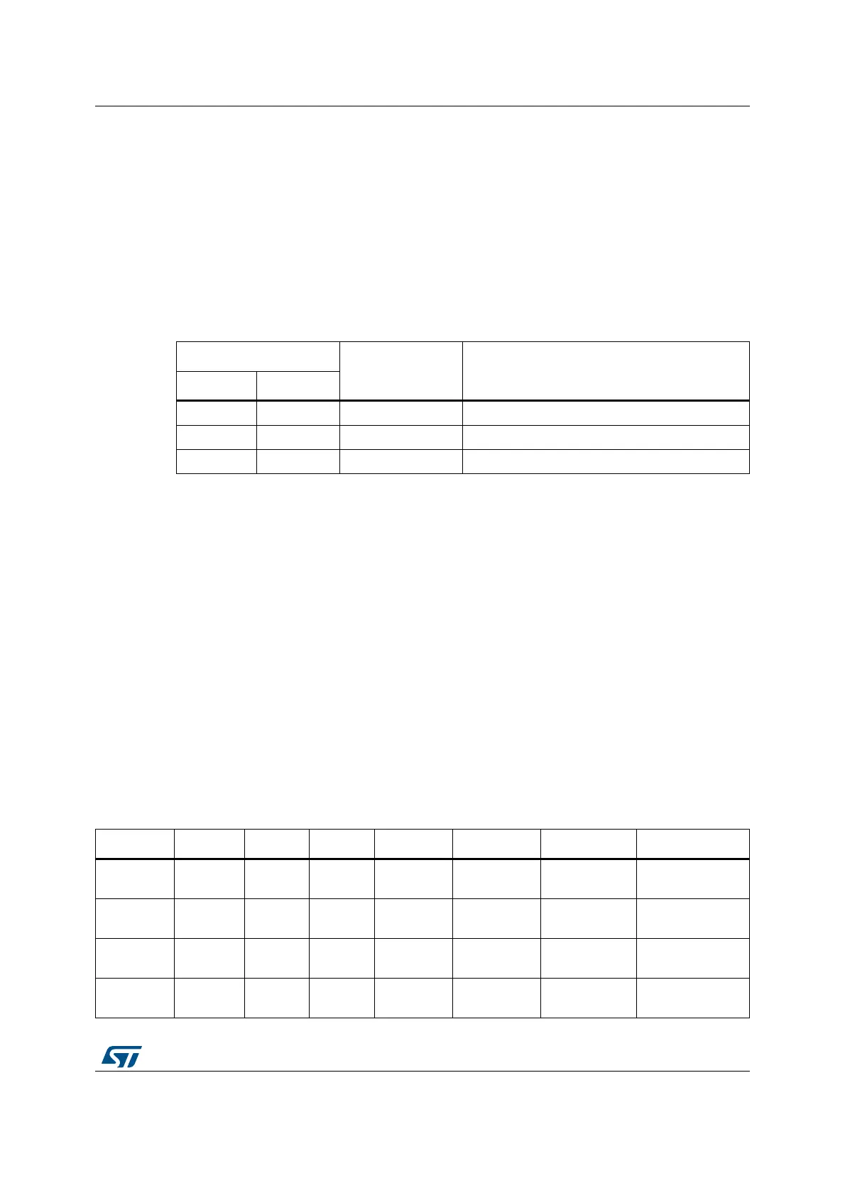
In the STM32F410, three different boot modes can be selected through the BOOT[1:0] pins
as shown in Table 2.
The values on the BOOT pins are latched on the 4th rising edge of SYSCLK after a reset. It
is up to the user to set the BOOT1 and BOOT0 pins after reset to select the required boot
mode.
BOOT0 is a dedicated pin while BOOT1 is shared with a GPIO pin. Once BOOT1 has been
sampled, the corresponding GPIO pin is free and can be used for other purposes.
The BOOT pins are also resampled when the device exits the Standby mode. Consequently,
they must be kept in the required Boot mode configuration when the device is in the Standby
mode. After this startup delay is over, the CPU fetches the top-of-stack value from address
0x0000 0000, then starts code execution from the boot memory starting from 0x0000 0004.
Note: When the device boots from SRAM, in the application initialization code, you have to
relocate the vector table in SRAM using the NVIC exception table and the offset register.
Embedded bootloader
The embedded bootloader mode is used to reprogram the Flash memory using interfaces
that depend on the package (refer to Table 3):
Table 2. Boot modes
Boot mode selection pins
Boot mode Aliasing
BOOT1 BOOT0
x 0 Main Flash memory Main Flash memory is selected as the boot space
0 1 System memory System memory is selected as the boot space
1 1 Embedded SRAM Embedded SRAM is selected as the boot space
Table 3. Embedded bootloader interfaces
Package USART1 USART2 I2C1 I2C2 I2C4 FM+ SPI1 SPI3
WLCSP36 X PA2/PA3 PB6/PB7 X PB10/PB3
PA15/PA5/
PB4/PB5
X
UFQFPN48 PA9/PA10 PA2/PA3 PB6/PB7 X PB14/PB15
PA4/PA5/
PA6/PA7
X
LQFP64 PA9/PA10 PA2/PA3 PB6/PB7 PB10/PB11 PB14/PB15
PA4/PA5/
PA6/PA7
PB12/PB13/
PC2/PC3
UFBGA64 PA9/PA10 PA2/PA3 PB6/PB7 PB10/PB11 PB14/PB15
PA4/PA5/
PA6/PA7
PB12/PB13/
PC2/PC3