Fast-mode Plus Inter-integrated circuit (FMPI2C) interface RM0401
526/771 RM0401 Rev 3
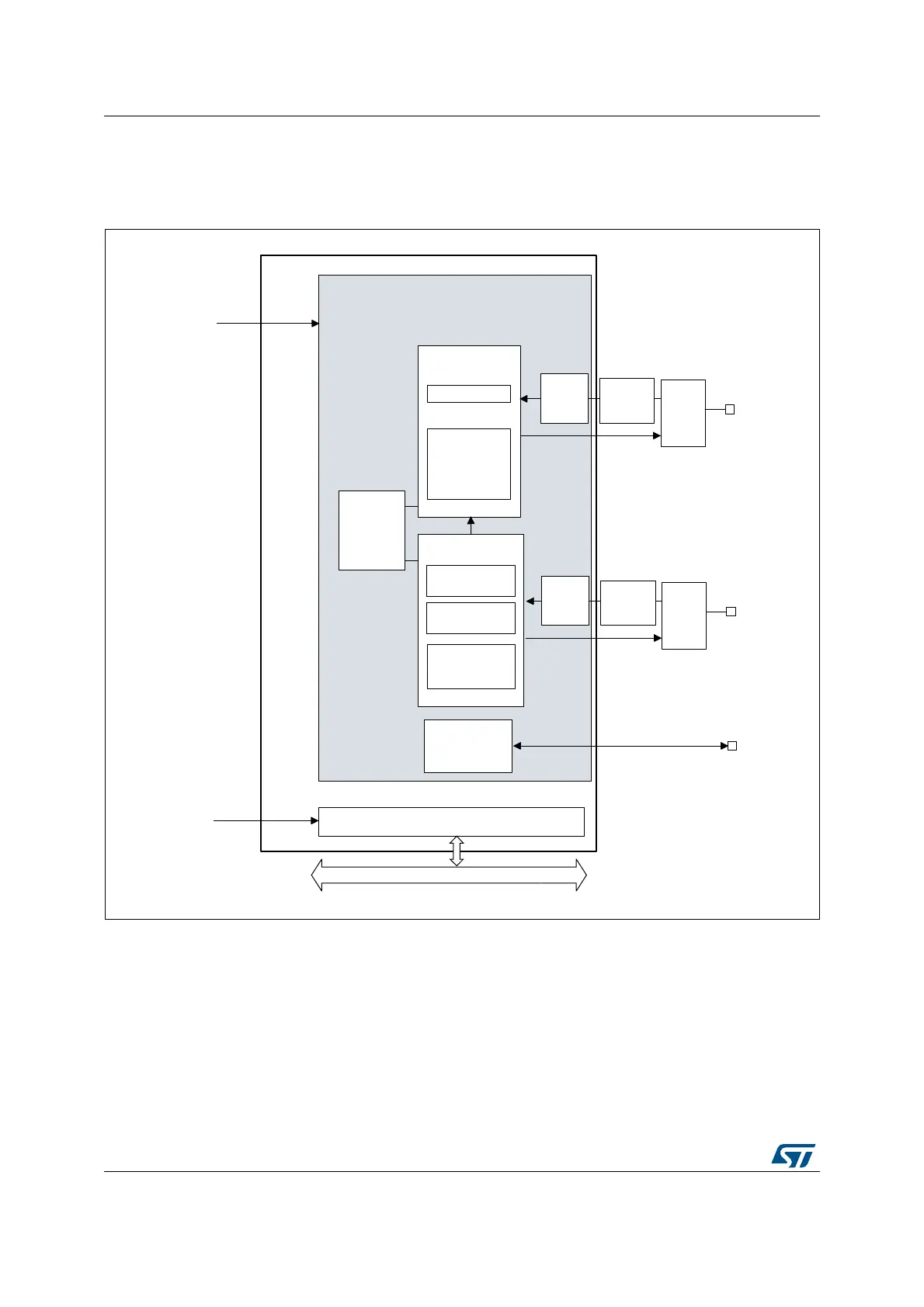
22.4.1 FMPI2C block diagram
The block diagram of the FMPI2C interface is shown in Figure 177.
Figure 177. FMPI2C block diagram
The FMPI2C is clocked by an independent clock source which allows to the FMPI2C to
operate independently from the PCLK frequency.
For I2C I/Os supporting 20 mA output current drive for Fast-mode Plus operation, the driving
capability is enabled through control bits in the system configuration controller (SYSCFG).
Refer to Section 22.3: FMPI2C implementation.
06Y9
,&&/.
:DNHXS
RQ
DGGUHVV
PDWFK
60%86
3(&
JHQHUDWLRQ
FKHFN
6KLIWUHJLVWHU
'DWDFRQWURO
60%XV
7LPHRXW
FKHFN
&ORFNFRQWURO
0DVWHUFORFN
JHQHUDWLRQ
6ODYHFORFN
VWUHWFKLQJ
60%XV$OHUW
FRQWURO
VWDWXV
'LJLWDO
QRLVH
ILOWHU
,&B6&/
,&B60%$
5HJLVWHUV
$3%EXV
*3,2
ORJLF
$QDORJ
QRLVH
ILOWHU
'LJLWDO
QRLVH
ILOWHU
,&B6'$
*3,2
ORJLF
$QDORJ
QRLVH
ILOWHU
,FBSFON
,FBNHUBFN
3&/.