RL78/G10 CHAPTER 6 TIMER ARRAY UNIT
R01UH0384EJ0311 Rev. 3.11 220
Dec 22, 2016
Figure 6-82. Example of Set Contents of Registers for Multiple PWM Output Function (Slave Channel)
(Output Two Types of PWMs) (2/2)
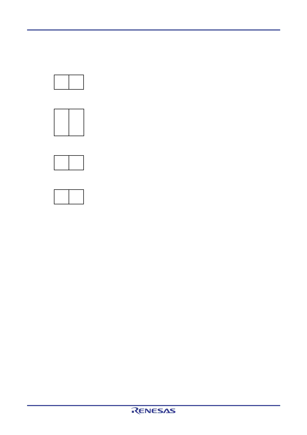
(b) Timer output register 0 (TO0)
Bit q Bit p
TO0
TO0q
1/0
TO0p
1/0
0: Outputs 0 from TO0p or TO0q.
1: Outputs 1 from TO0p or TO0q.
(c) Timer output enable register 0 (TOE0)
Bit q Bit p
TOE0
TOE0q
1/0
TOE0p
1/0
0: Stops the TO0p or TO0q output operation by counting operation (the level set in the TO0p or
TO0q bit is output from the TO0p or TO0q pin).
1: Enables the TO0p or TO0q output operation by counting operation (output from the TO0p or
TO0q pin is toggled).
(d) Timer output level register 0 (TOL0)
Bit q Bit p
TOL0
TOL0q
1/0
TOL0p
1/0
0: Positive logic output (active-high)
1: Negative logic output (active-low)
(e) Timer output mode register 0 (TOM0)
Bit q Bit p
TOM0
TOM0q
1
TOM0p
1
1: Sets the slave channel output mode.
Remark p: Channel number of slave channel 1, q: Channel number of slave channel 2
0 < p < q ≤ 3 (Where p and q are consecutive integers greater than 0)

 Loading...


