RL78/G15 CHAPTER 5 CLOCK GENERATOR
R01UH0959EJ0110 Rev.1.10 Page 135 of 765
Mar 7, 2023
5.3.2 System clock control register (CKC)
This register is used to select a main system clock.
The CKC register can be set by a 1-bit or 8-bit memory manipulation instruction.
Reset signal generation sets this register to 00H.
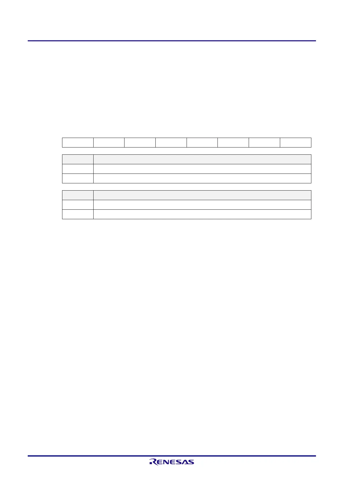
Figure 5-3. Format of System Clock Control Register (CKC)
Address: FFFA4H After reset: 00H R/W
Note 1
Symbol 7 6
□
5
□
4 3 2 1 0
CKC 0 0 MCS MCM0 0 0 0 0
MCS Status of Main system clock (f
MAIN
)
0 High-speed on-chip oscillator clock (f
IH
)
1 High-speed system clock (f
MX
)
MCM0 Main system clock (f
MAIN
) operation control
0 Selects the high-speed on-chip oscillator clock (f
IH
) as the main system clock (f
MAIN
)
1 Selects the high-speed system clock (f
MX
) as the main system clock (f
MAIN
)
Note 1. Bit 5 is read-only.
Caution 1. Be sure to set bit 0 to 3, 6, and 7 to 0.
Caution 2. Do not select the high-speed system clock (f
MX
) as the main system clock (f
MAIN
) before the
oscillation stabilization time has elapsed after oscillation of f
MX
is started.
Caution 3. When the main system clock (f
MAIN
) is changed, the peripheral hardware clock also changes at the
same time. Only change f
MAIN
after stopping all peripheral functions and setting the MCM0 bit.
 Loading...


