RL78/G15 CHAPTER 12 SERIAL ARRAY UNIT
R01UH0959EJ0110 Rev.1.10 Page 391 of 765
Mar 7, 2023
12.3.14 Input switch control register (ISC)
The ISC1 and ISC0 bits in the ISC register are used to handle the combination of the external interrupt and the timer
array unit at the time of baud rate correction of UART0.
When bit 0 is set to 1, the input signal of the serial data input (RxD0) pin is selected as an external interrupt (INTP0) that
can be used to detect a wakeup signal.
When bit 1 is set to 1, the input signal of the serial data input (RxD0) pin is selected as a timer input, so that wake up
signal can be detected, the low width of the break field, and the pulse width of the sync field can be measured by the
timer.
The ISC register can be set by a 1-bit or 8-bit memory manipulation instruction.
The value of the ISC register is 00H following a reset.
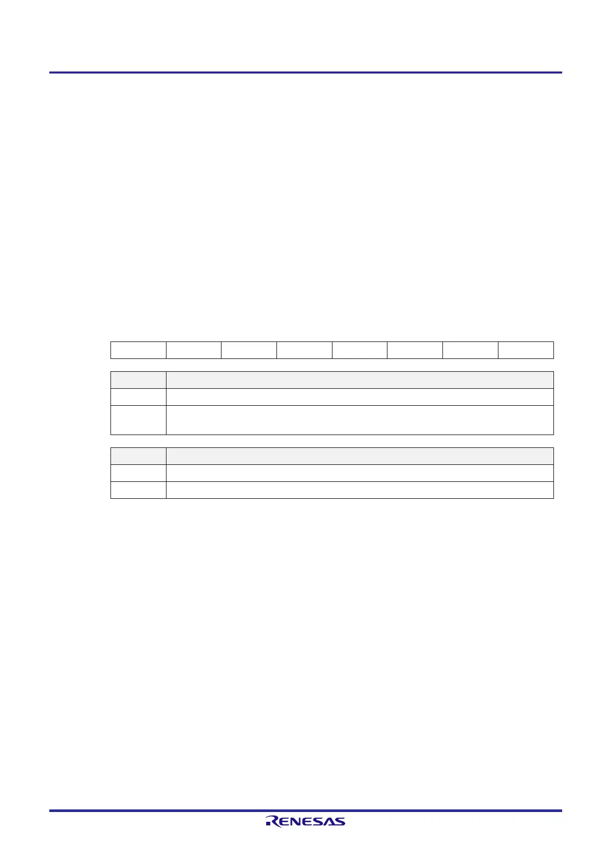
Figure 12-17. Format of Input Switch Control Register (ISC)
Address: F0073H After reset: 00H R/W
Symbol 7 6 5 4 3 2 1 0
ISC 0 0 0 0 0 0 ISC1 ISC0
ISC1 Switching the channel 7 of the timer array unit
0 Select the input signal on TI01 pin as the timer input (normal operation)
1
Select the input signal on RxD0 pin as the timer input (Detection of the wake-up signal and pulse-width-
measurement for baud rate correction)
ISC0 Switching the external interrupt (INTP0)
0 Select the input signal on INTP0 pin as the external interrupt input (normal operation)
1 Select the input signal on RxD0 pin as the external interrupt input (detection of the wake-up signal)
Caution Be sure to clear bits 7 to 2 to 0.
 Loading...


