RL78/G15 CHAPTER 5 CLOCK GENERATOR
R01UH0959EJ0110 Rev.1.10 Page 142 of 765
Mar 7, 2023
5.3.6 Peripheral enable register 0 (PER0)
This register is used to enable or disable supplying the clock to the peripheral hardware. Clock supply to the hardware
that is not used is also stopped so as to decrease the power consumption and noise.
To use the peripheral functions below, which are controlled by this register, set (1) the bit corresponding to each function
before specifying the initial settings of the peripheral functions.
●
12-bit Interval timer
●
A/D converter
●
Comparator
●
IICA Serial interface IICA
●
Serial array unit
●
Timer array unit
The PER0 register can be set by a 1-bit or 8-bit memory manipulation instruction.
Reset signal generation clears these registers to 00H.
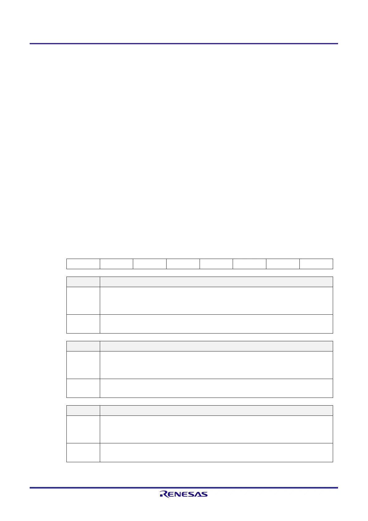
Figure 5-7. Format of Peripheral Enable Register 0 (PER0) (1/2)
Address: F00F0H After reset: 00H R/W
Symbol
□
7
□
6
□
5
□
4 3
□
2 1
□
0
PER0 TMKAEN
Note 1
CMPEN
Note 1
ADCEN IICA0EN
Note 1
0 SAU0EN 0 TAU0EN
TMKAEN Control of 12-bit interval timer input clock supply
0 Stops input clock supply.
●
SFR used by the 12-bit interval timer cannot be written.
●
The 12-bit interval timer is in the reset status.
1 Enables input clock supply.
●
SFR used by the 12-bit interval timer can be read and written.
CMPEN Control of comparator input clock supply
0 Stops input clock supply.
●
SFR used by the comparator cannot be written.
●
The comparator is in the reset status.
1 Enables input clock supply.
●
SFR used by the comparator can be read and written.
ADCEN Control of A/D converter input clock supply
0 Stops input clock supply.
●
SFR used by the A/D converter cannot be written.
●
The A/D converter is in the reset status.
1 Enables input clock supply.
●
SFR used by the A/D converter can be read and written.
 Loading...


