RL78/G15 CHAPTER 8 CLOCK OUTPUT/BUZZER OUTPUT CONTROLLER
R01UH0959EJ0110 Rev.1.10 Page 309 of 765
Mar 7, 2023
8.3.2 Registers controlling port functions of clock output/buzzer output pin
Using the port pin for the clock output/buzzer output controller requires setting of the registers that control the port
function multiplexed on the clock output/buzzer output pin (PCLBUZ0 pin): (port mode registers 0, 4 (PM0, PM4), port
registers 0, 4 (P0, P4), port mode control register 0 (PMC0), peripheral I/O redirection register 3 (PIOR3)).
For details on the registers that control the port functions, see 4.3.1 Port mode registers 0, 2, 4, 12 (PM0, PM2, PM4,
PM12), 4.3.2 Port registers 0, 2, 4, 12, 13 (P0, P2, P4, P12, P13), 4.3.5 Port mode control registers 0, 2 (PMC0,
PMC2), and 4.3.6 Peripheral I/O redirection registers 0 to 3 (PIOR0 to PIOR3).
When you intend to use the PCLBUZ0 pin, set the corresponding bits in the port mode register (PM0) and port mode
control register 0 (PMC0) to 0 and the corresponding bits in the port register (P0) and port output mode register (POM0)
to 0.
For details, see 4.5.3 Register setting examples for used port and alternate functions.
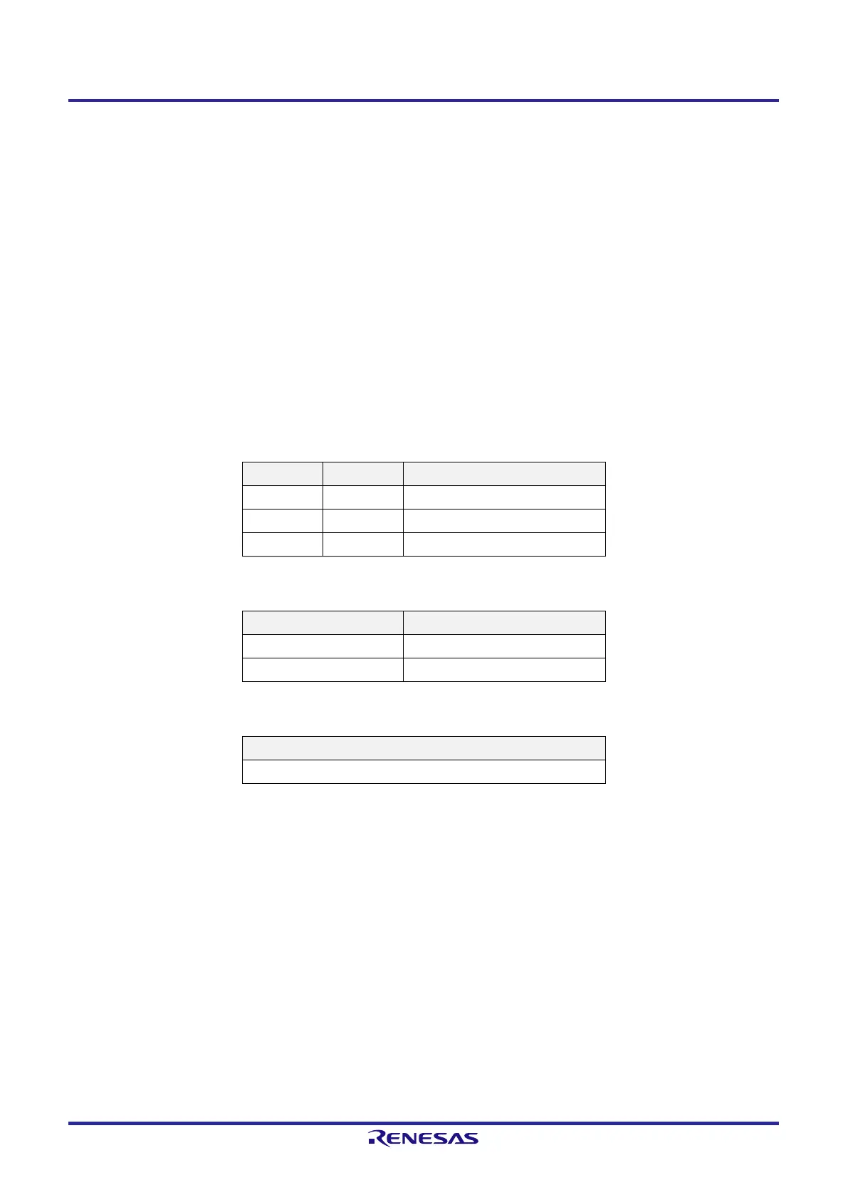
The table below lists the clock output/buzzer output pins set by the PIOR3 register.
16- and 20-Pin Products
PIOR31 PIOR30 Clock Output/Buzzer Output Pin
0 0 P02 (initial value)
0 1 P40
1 0 P06
10-Pin Products
PIOR30 Clock Output/Buzzer Output Pin
0 P02 (initial value)
1 P40
8-Pin Products
Clock Output/Buzzer Output Pin
Fixed to pin P40
 Loading...


